Precision in TGV Glass Wafers
Through Glass Via technology creates vertical electrical interconnects through a glass substrate, allowing electrical signals to pass between the front and back sides of the wafer while supporting high-density three-dimensional packaging.
TGVGlass combines glass microvia formation with via metallization, microstructure fabrication, RDL routing, wafer bonding, dicing and testing. The platform supports both wafer-level and panel-level development for semiconductor, MEMS, optical communication, display and other advanced packaging applications.
From initial TGV substrate fabrication to integrated glass-based packaging, wafers can be customized according to material, thickness, via diameter, via profile and final device requirements.
TGV Glass Wafer Capability
| Project | Capability |
|---|---|
| Wafer Size | 2 in., 4 in., 6 in., 8 in., 12 in. |
| Panel Size | ≤510 × 510 mm |
| Glass Materials | Borosilicate, high-aluminosilicate, alkali-free glass, quartz and other technical glasses |
| Glass Thickness | 100–5000 µm |
| Microvia Diameter | <20 µm |
| Tolerance | Within ±3 µm |
| Via Profiles | Vertical, oblique, waist-shaped |
| Metallized Via Diameter | <30 µm |
| Via Types | Through vias and blind vias |
| Metallization | Paste filling, electroplating and combined filling processes |
TGV Glass Wafer Solutions
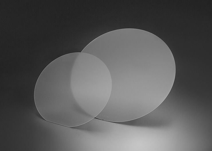
TGV Glass Wafers
Precision glass wafers with through-glass microvias for wafer-level vertical interconnection and advanced packaging. Available from 2 in. to 12 in. in multiple technical glass materials.
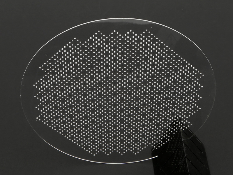
Metallized TGV Wafers
TGV wafers with high-density conductive vias for vertical electrical interconnection. Through vias and blind vias below 30 µm can be metallized according to device requirements.

Panel-Level TGV Substrates
Large-format glass substrates up to 510 × 510 mm for applications requiring panel-level processing and higher substrate utilization.
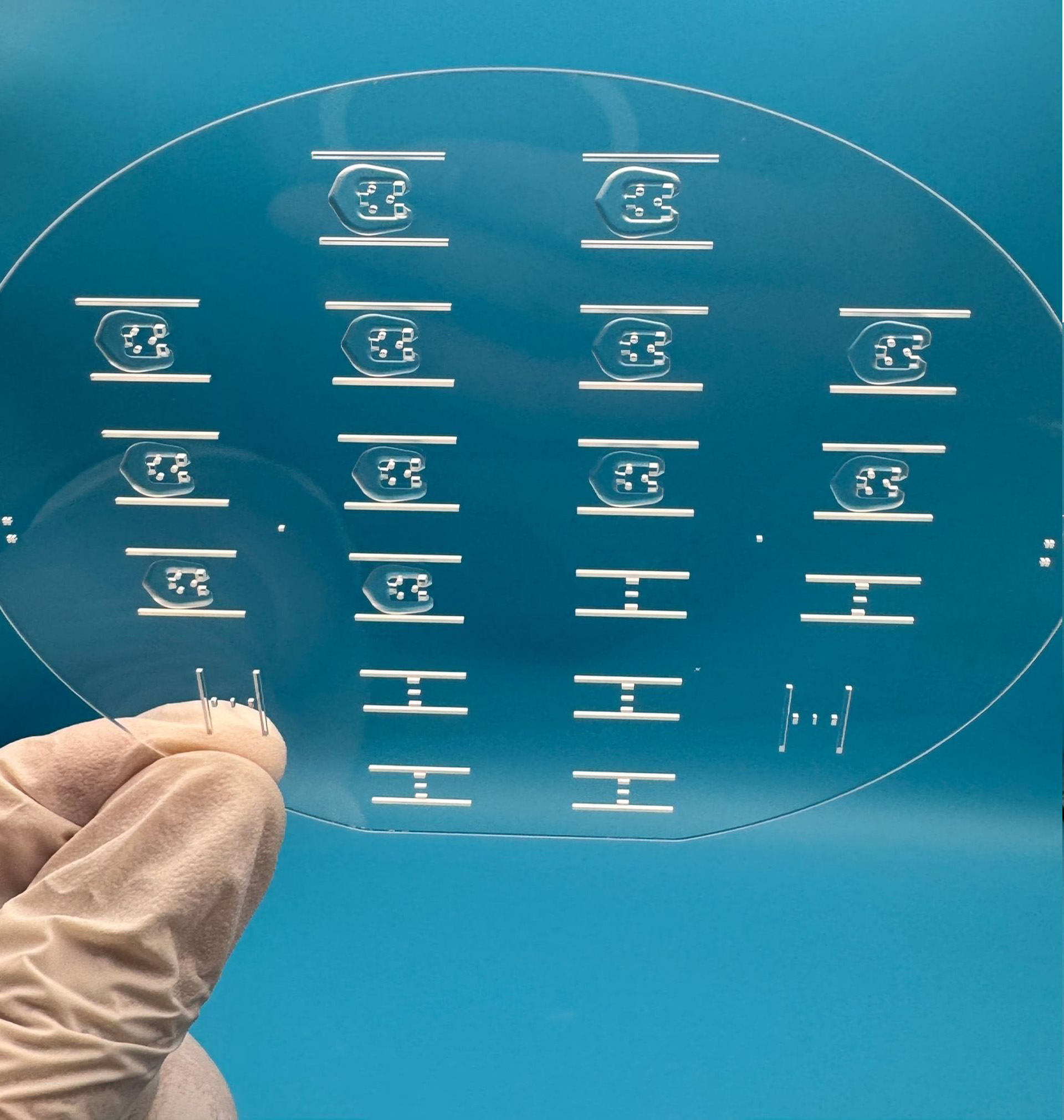
Custom TGV Structures
Vertical, oblique and waist-shaped microvias can be fabricated according to the required glass thickness, via geometry and packaging architecture.
Need Help?
Send us your glass material, wafer size, via geometry, and metallization requirements for process evaluation.
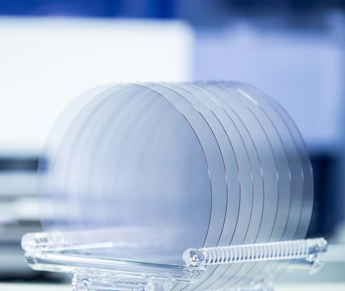
Custom TGV Glass Wafers
TGVGlass manufactures glass wafers according to customer device layouts and packaging requirements. Substrate material, wafer diameter, glass thickness, via diameter, via profile and metallization can all be customized.
Our TGV platform supports borosilicate glass, high-aluminosilicate glass, alkali-free glass and quartz, with wafer formats from 2 in. to 12 in. and panel substrates up to 510 × 510 mm.
TGV Fabrication Capabilities
- Glass microvia formation — batch via diameters below 20 µm
- Precision control — tolerances within ±3 µm
- Via profiles — vertical, oblique and waist-shaped
- Microvia metallization — through and blind vias below 30 µm
- Surface routing — TGV substrate and multilayer RDL routing
- Wafer integration — bonding, dicing and performance testing
Applications
TGV glass wafers for RF, MEMS, optical communication, display, vacuum, and advanced semiconductor packaging.
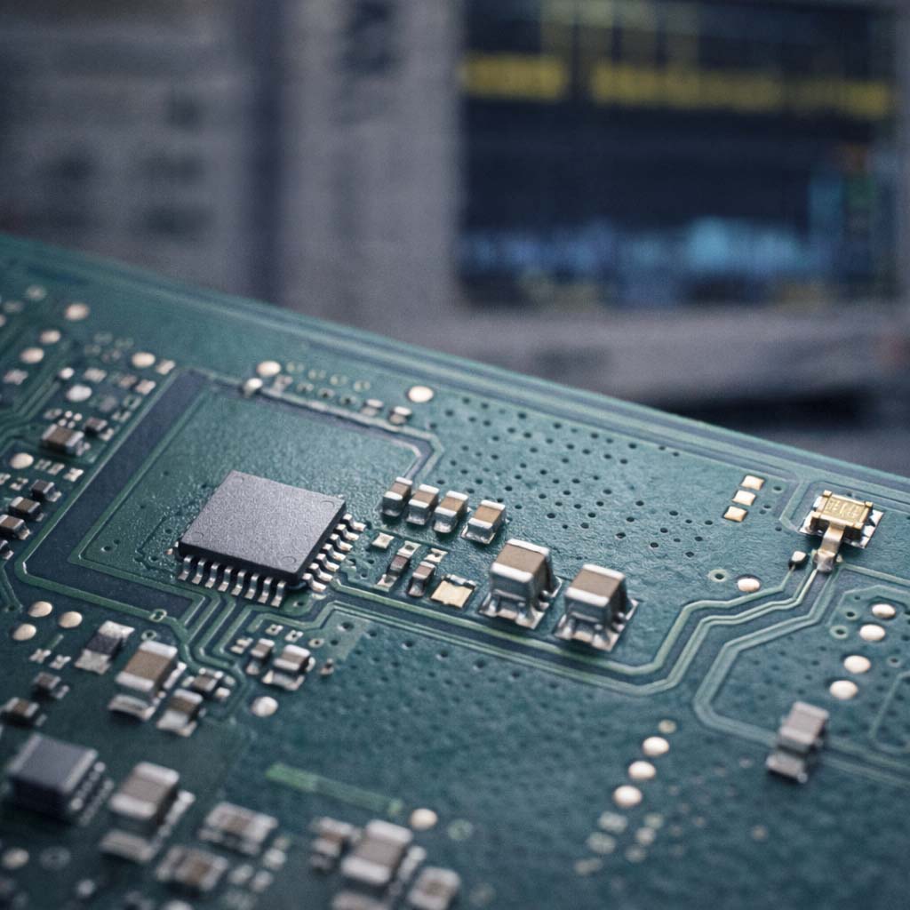
RF & High-Frequency Devices
TGV glass substrates provide high-density vertical interconnect structures for RF chips and other high-frequency packaging architectures requiring compact electrical routing.
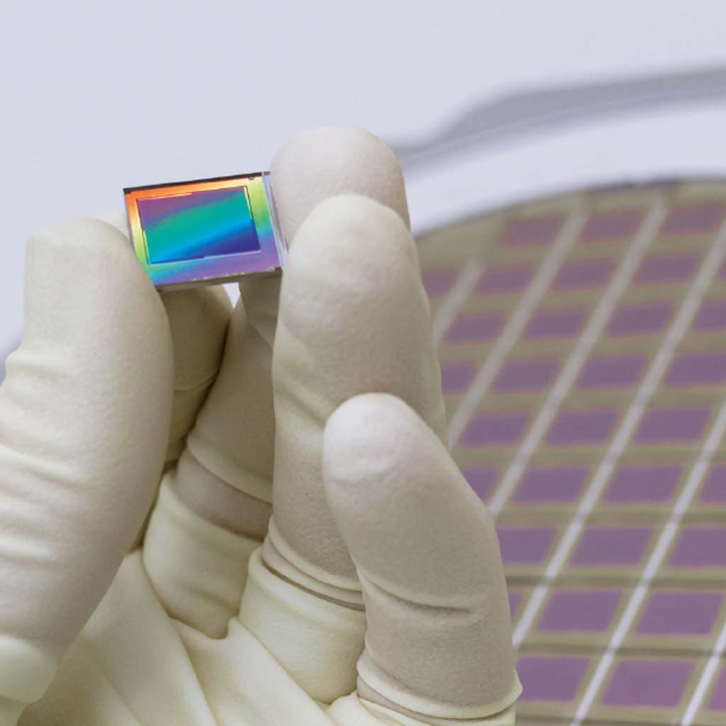
MEMS & Sensors
TGV wafers integrate vertical interconnects with glass-based packaging structures for MEMS sensors, gyroscopes and other wafer-level sensor devices.
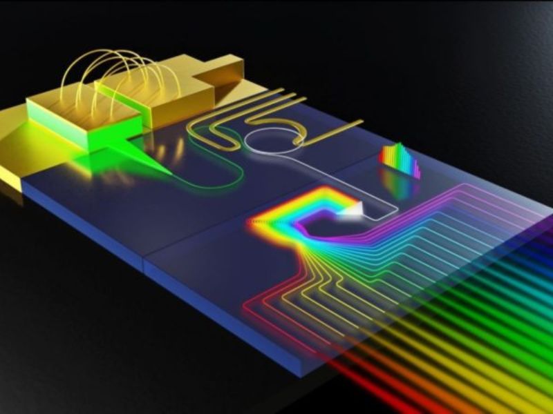
CPO & Optical Communication
Glass-based vertical interconnects and precision microstructures are used in CPO and optical communication packaging where electrical and optical functions must be integrated within a compact substrate.
Mini-LED & Display
TGV substrates support high-density interconnection for Mini-LED and other display-related packaging applications requiring large numbers of vertical electrical connections.
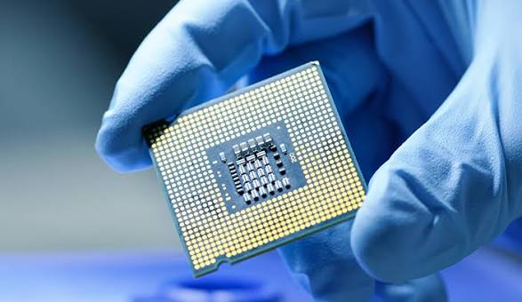
Vacuum & Advanced Semiconductor Packaging
Glass-based TGV technology integrates with wafer bonding and other packaging processes for vacuum electronic devices and advanced semiconductor packages.
Connect with Our Experts
We’re Here to Help
Our engineers review your drawing, material, tolerances, and target quantity before quotation.
Request a Process Evaluation
Tell us your glass material, wafer or panel size, substrate thickness, via diameter, via quantity, metallization requirements and final application.