Conductive Silicon TGV Wafer Architecture
Conductive silicon TGV is a heterogeneous wafer structure formed by integrating glass and silicon within the same substrate.
Unlike a conventional glass TGV wafer based primarily on metal-filled vias, the conductive silicon structure uses patterned silicon regions together with insulating glass to create electrical feedthrough and packaging structures.
This architecture is particularly suited to devices requiring electrical isolation, hermetic sealing and wafer-level integration.
Conductive Silicon TGV Structures
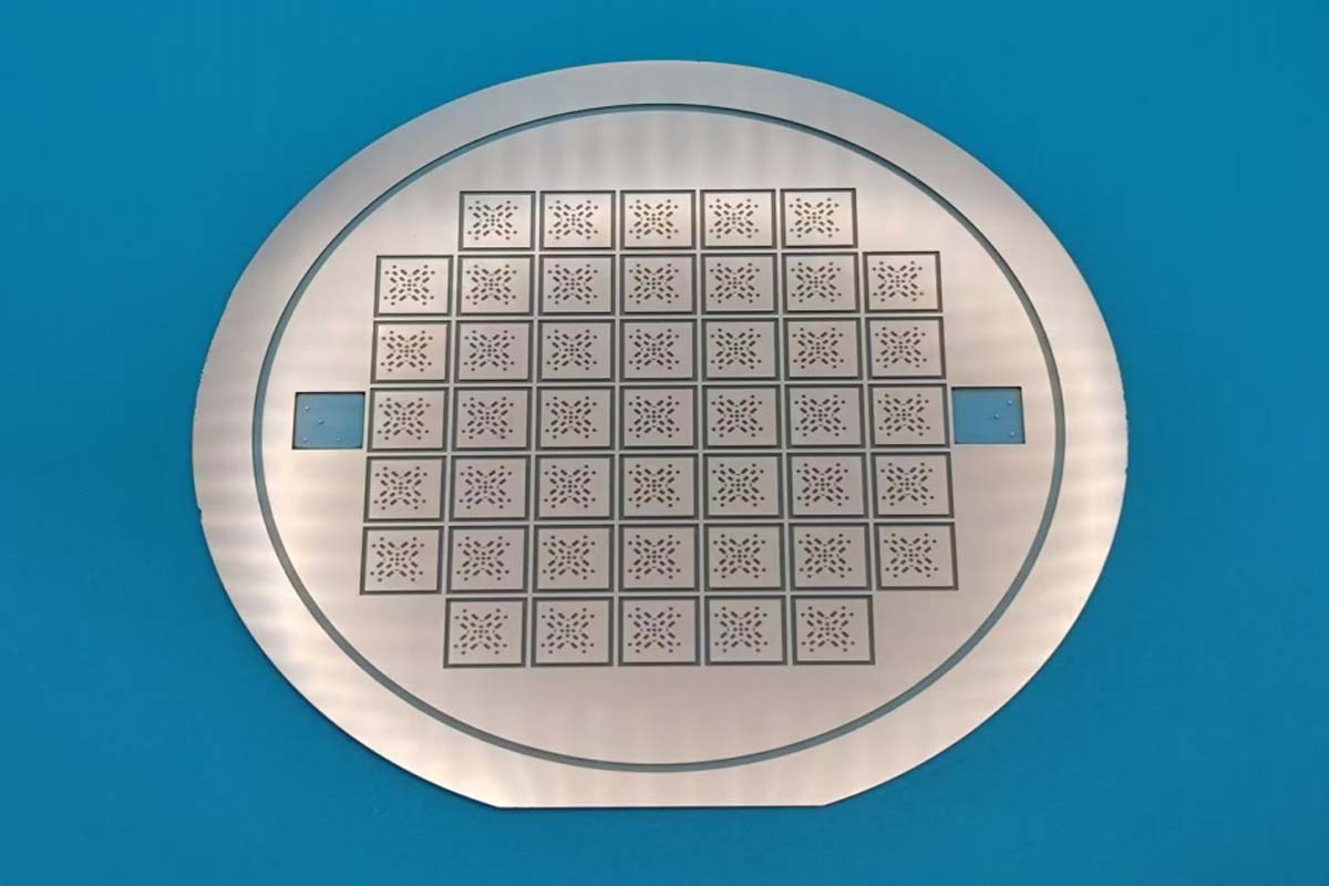
Heterogeneous Glass–Silicon Wafers
Glass and silicon are integrated into a wafer-level heterogeneous substrate for electrical interconnection and hermetic packaging.
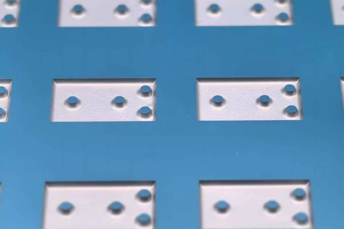
Conductive Silicon Cavities
Silicon regions can be processed into cavity structures for devices requiring defined packaging spaces or sealed internal volumes.
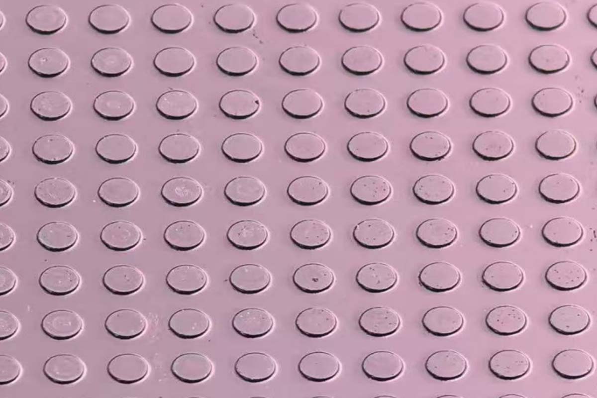
Silicon Microstructures
Silicon etching can be combined with the glass–silicon structure to create application-specific device and packaging geometries.
Hermetic Feedthrough Structures
Conductive silicon regions provide electrical paths through an insulating glass structure while supporting hermetic package designs.
Need Help?
If your device requires electrical feedthroughs, glass–silicon integration or hermetic wafer-level packaging, send us your device structure and packaging requirements for evaluation.
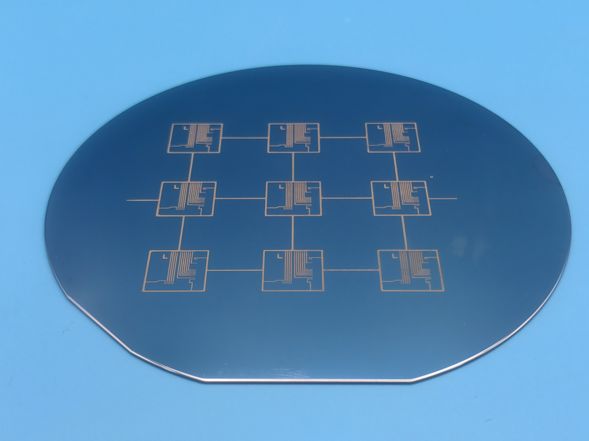
Custom Conductive Silicon TGV Wafers
Conductive silicon TGV wafers can be customized according to the required silicon structure, glass isolation region, cavity layout and device packaging architecture.
The glass–silicon heterogeneous structure is formed using high-temperature glass reflow technology, enabling glass and patterned silicon to be integrated within the same wafer.
Typical Project Requirements
- Glass / silicon heterogeneous structures
- Conductive silicon feedthroughs
- Electrical isolation regions
- Silicon cavities
- Custom silicon patterns
- Hermetic packaging structures
- Wafer-level device layouts
High Isolation & Hermetic Packaging
One of the key characteristics of conductive silicon TGV is the separation of conductive silicon regions by insulating glass.
This makes the structure suitable for devices requiring electrical isolation between different conductive areas while maintaining electrical paths through the wafer.
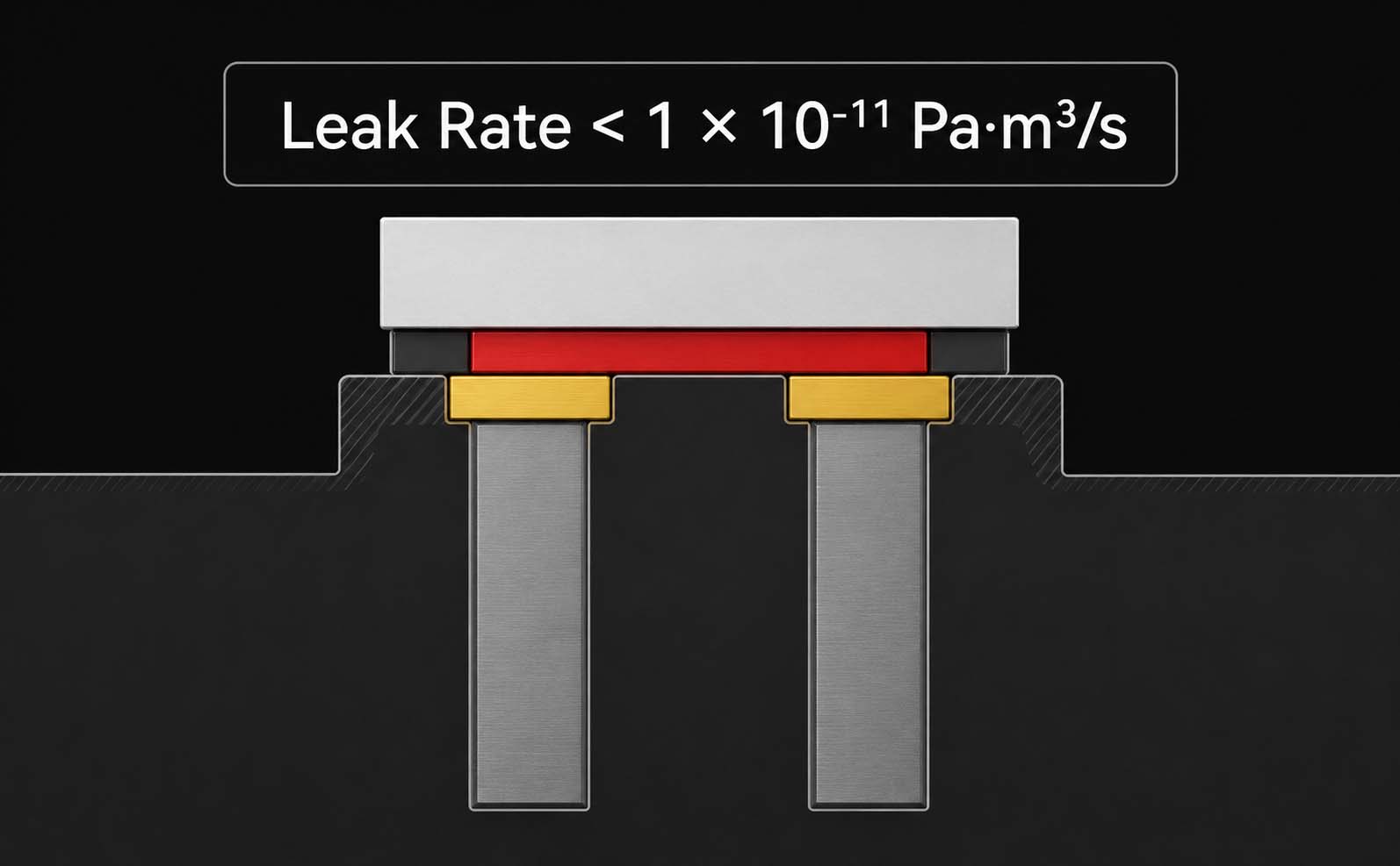
For vacuum and hermetic packaging structures, demonstrated helium leak rates are below:
1 × 10⁻¹¹ Pa·m³/s
Applications
Glass–silicon heterogeneous wafers for sealed sensing, resonator, MEMS and vacuum-device packaging.
MEMS Gyroscopes
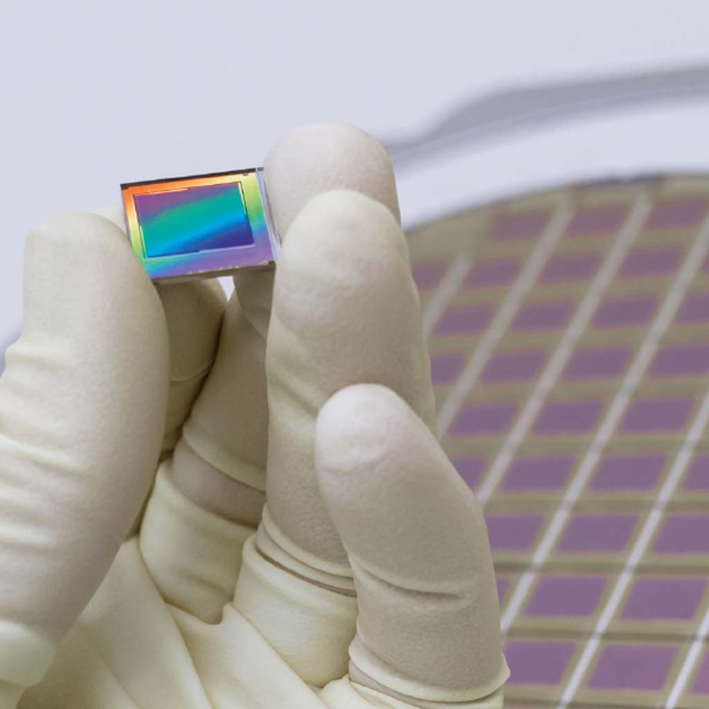
Conductive silicon TGV wafers can be used in wafer-level MEMS gyroscope packaging requiring electrical feedthroughs, isolation and sealed device structures.
Resonators
Glass–silicon heterogeneous wafers can support resonator packaging where conductive silicon structures and electrically isolating glass regions are required within the same substrate.
Gas Sensors
Conductive silicon TGV structures can be used in sealed gas-sensor wafer architectures requiring cavities, electrical connections and controlled package structures.
Vacuum Devices
The high-hermeticity glass–silicon structure is suitable for vacuum device packaging where electrical feedthroughs must pass through a sealed package boundary.
Why Conductive Silicon TGV?
Electrically insulating glass, patterned conductive silicon, and hermetic wafer bonding are integrated in one structure.
Glass–Silicon Integration
Glass and silicon are combined within a single heterogeneous wafer structure rather than used only as separate bonded substrates.
Electrical Isolation
Insulating glass regions provide separation between conductive silicon structures.
High Hermeticity
The glass–silicon structure supports hermetic and vacuum packaging applications, with demonstrated helium leak rates below 1×10⁻¹¹ Pa·m³/s.
Custom Wafer Structures
Silicon patterns, cavities, conductive regions and glass isolation structures can be configured according to the device and package design.
Frequently Asked Questions
It is a glass–silicon heterogeneous wafer in which conductive silicon structures are integrated with electrically insulating glass to create functional feedthrough and packaging structures.
Conventional TGV typically uses vias formed in a glass substrate and subsequently metallized. Conductive silicon TGV instead integrates patterned conductive silicon regions with glass to create a heterogeneous wafer structure.
Yes. The technology is intended for high-isolation and high-hermeticity packaging structures. Demonstrated helium leak rates are below 1×10⁻¹¹ Pa·m³/s.
Typical applications include MEMS gyroscopes, resonators, gas sensors and vacuum devices.
Yes. Silicon patterns, cavities and glass–silicon layouts can be developed according to the device structure and packaging requirements.
Connect with our experts
We’re here to help
Our engineers review your drawing, material, tolerances, and target quantity before quotation.
Request a Process Evaluation
Tell us about the substrate, dimensions, tolerance, quantity, processing, bonding, routing, or packaging requirements.