What Is a Glass Wafer?
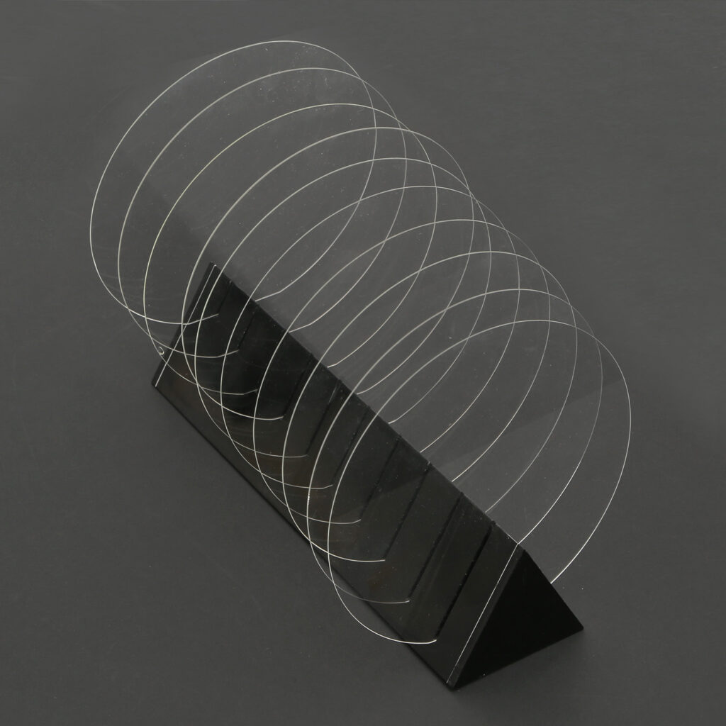
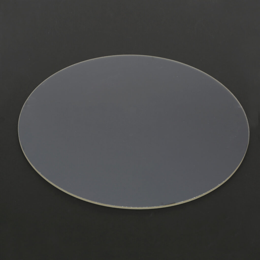
A glass wafer is a precision glass substrate used in semiconductor and MEMS manufacturing where electrical insulation, thermal stability, optical transmission, and compatibility with wafer-level processing are required.
Unlike silicon wafers, glass wafers combine electrical isolation with optical transparency and chemical resistance. Depending on the application, borosilicate or quartz glass is selected to match the required bonding method, processing temperature, optical wavelength, and material purity.
Customer Requirements
Selecting the right glass wafer depends heavily on the downstream process. MEMS packaging may require thermal expansion behavior compatible with silicon for anodic bonding. Semiconductor processing may place greater emphasis on chemical purity and CMOS compatibility, while optical and high-temperature applications require suitable transmission and thermal stability.
Choosing the wafer material according to the final process helps reduce bonding, contamination, and thermal-mismatch issues.
Glass Wafer Materials
Two technical glass platforms matched to different bonding, purity, thermal, and optical requirements.
| Material | Key Properties | Typical Applications |
|---|---|---|
| BOROFLOAT® 33 Glass | Coefficient of thermal expansion (CTE) adapted to silicon, good optical transmission, high chemical resistance, and mechanical strength | MEMS, wafer-level packaging, anodic bonding, semiconductor processing, optics |
| Semiconductor-Grade Quartz | High chemical purity, low CTE, low OH content, UV and IR transmission | Semiconductor processing, solar, thin-film coating, optical, and high-temperature applications |
Need Help?
If you are unsure which glass wafer material is suitable for your process, send us your application and processing requirements for evaluation.
Glass Wafer Material Options: BOROFLOAT® 33 vs. Quartz
Compare the silicon-compatible borosilicate platform with high-purity semiconductor-grade quartz.
BOROFLOAT® 33 Glass Wafers
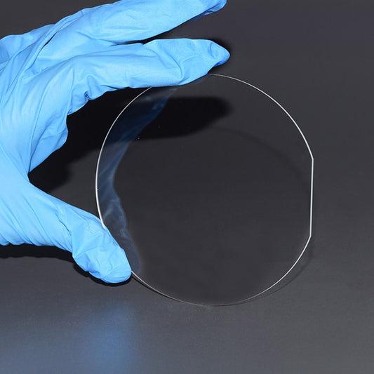
BOROFLOAT® 33 glass wafers are widely used in semiconductor and MEMS applications. Their coefficient of thermal expansion is adapted to silicon, making the material particularly suitable for anodic bonding and wafer-level packaging.
The wafers provide broad optical transmission, high chemical resistance, mechanical strength, and compatibility with high-temperature processing. They can be used as MEMS encapsulation wafers, semiconductor-processing blanks, and optical substrates.
Semiconductor-Grade Quartz Wafers
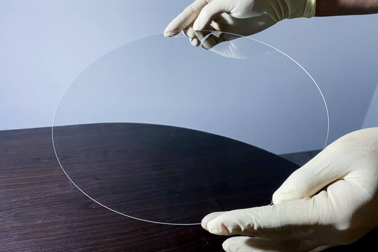
Quartz wafers provide a high-purity substrate for semiconductor processing, solar applications, industrial applications, and thin-film coatings. The amorphous quartz combines high chemical purity with excellent mechanical and optical properties.
Its low coefficient of thermal expansion and low OH content support high-temperature processing while maintaining good transmission in both UV and IR regions.
Applications
Glass and quartz wafers selected around packaging, process purity, optical transmission, and thermal stability.
MEMS & Wafer-Level Packaging
BOROFLOAT® 33 wafers can be used as cap or encapsulation wafers for MEMS sensors and other devices manufactured using wafer-level packaging technology.
Semiconductor Processing
Both glass and quartz wafers can serve as blank substrates. Semiconductor-grade quartz is particularly suitable where high chemical purity and CMOS compatibility are required.
Optics, Solar & Thin-Film Coatings
Glass wafers can be used as optical substrates, while semiconductor-grade quartz supports solar, industrial, and thin-film applications requiring high purity and thermal stability.
Why Choose the Right Glass Wafer?
Match the material platform to the dominant bonding, purity, or thermal requirement of the application.
Silicon-Compatible Glass
BOROFLOAT® 33 provides thermal expansion behavior adapted to silicon, making it a practical choice for anodic bonding and MEMS packaging.
High-Purity Quartz
Semiconductor-grade quartz provides high chemical purity and CMOS compatibility for demanding semiconductor processes.
High-Temperature Compatibility
Both materials support high-temperature applications, while quartz combines low CTE and low OH content with UV and IR transmission.
Solutions for Common Wafer Requirements
Practical material routes for bonding, contamination control, optics, and elevated-temperature processing.
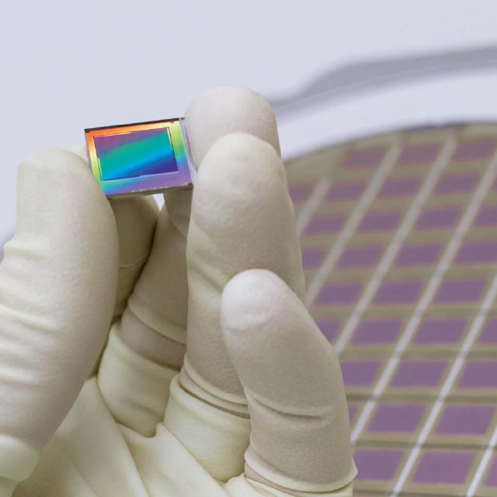
Anodic Bonding with Silicon
For MEMS structures requiring glass-to-silicon anodic bonding, BOROFLOAT® 33 provides a coefficient of thermal expansion suited to silicon-based assemblies.
High-Purity Semiconductor Processing
Where chemical purity and CMOS compatibility are primary requirements, semiconductor-grade quartz provides a suitable wafer substrate.
UV, IR & High-Temperature Applications
Quartz wafers combine low OH content, low thermal expansion, and transmission in the UV and IR for optical and high-temperature process environments.
Connect with Our Experts
We’re Here to Help
Tell us which wafer material you require and how it will be used. Our team can help evaluate BOROFLOAT® 33 glass or semiconductor-grade quartz for your semiconductor, MEMS, optical, solar, or thin-film application.
Quote Form
Send the material, wafer format, dimensional, processing, and quantity requirements for an initial product review.