Our Glass Microvia Formation Technologies
Terminology: a via is the hole itself, a microvia is a fine-diameter via, and TGV describes the complete through-glass interconnect structure and process.
Different glass materials, via geometries and packaging structures require different microvia formation methods. TGVGlass selects the processing route according to substrate material, thickness, via dimensions and required structure.
The appropriate process is selected according to the customer’s glass substrate and final packaging requirements.
- Laser-Induced EtchingUsed for precision glass microvia formation and high-density TGV structures.
- SandblastingSuitable for glass through holes, blind structures and other custom microstructures.
- Wet EtchingUsed for selected glass microstructures and via geometries according to material and design requirements.
- Dry EtchingAvailable for precision microstructure fabrication requiring controlled feature geometry.
Specifications
| Parameter | Capability |
|---|---|
| Wafer Size | 2 in., 4 in., 6 in., 8 in., 12 in. |
| Panel Size | ≤510 × 510 mm |
| Glass Materials | Borosilicate, high-aluminosilicate, alkali-free glass, quartz and other technical glasses |
| TGV Glass Thickness | 100–3000 µm |
| Batch Microvia Diameter | <20 µm |
| TGV Tolerance | Within ±3 µm |
| Via Structures | Through, blind, oblique, waist-shaped |
| Microvia Arrays | Custom layout |
| Process Routes | Laser-induced etching, sandblasting, wet etching, dry etching |
Glass Microvia Structures We Make
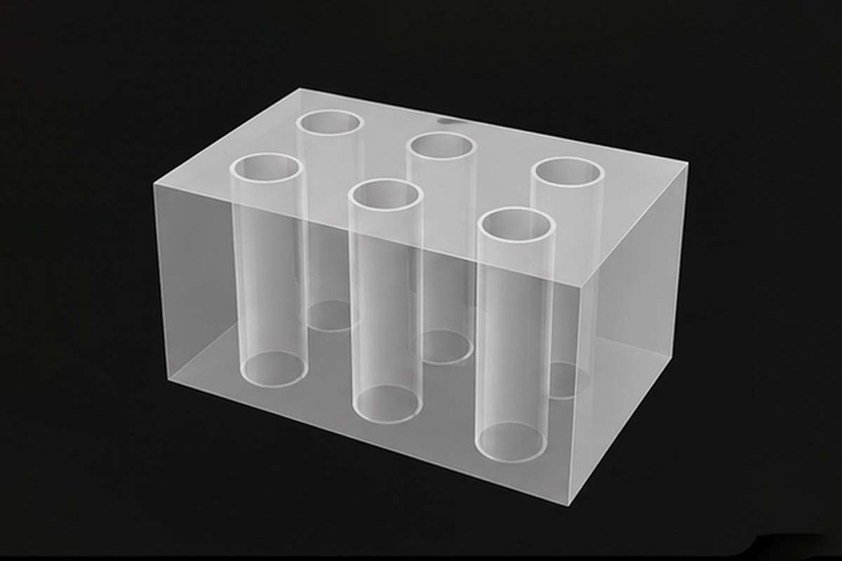
Glass Through Holes
Through-glass vias extend through the complete glass substrate and form the basic structure for vertical electrical interconnection in TGV packaging.
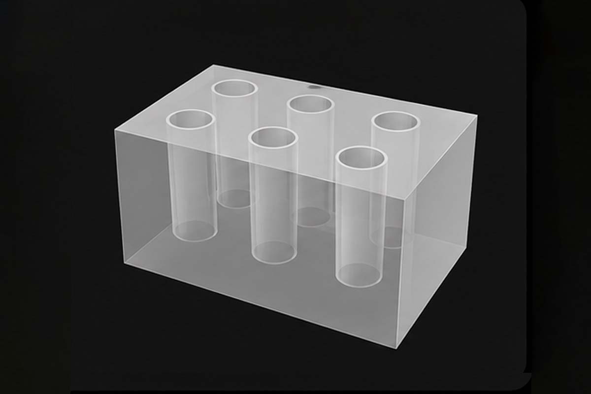
Glass Blind Holes
Blind vias terminate within the glass substrate rather than passing completely through it. They can be fabricated for selected microstructure and packaging designs.
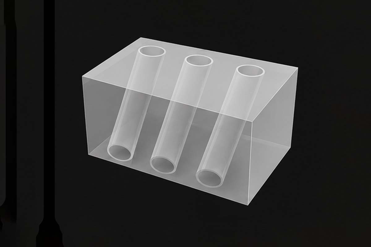
Oblique Glass Vias
Oblique vias provide an angled microstructure through or into the glass substrate where a conventional vertical via does not match the device architecture.
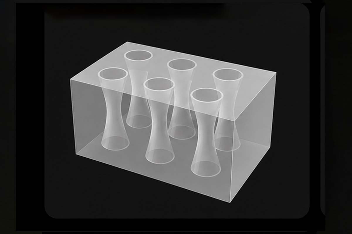
Waist-Shaped Vias
Waist-shaped vias use a narrowed internal profile and can be fabricated according to TGV structure and subsequent metallization requirements.
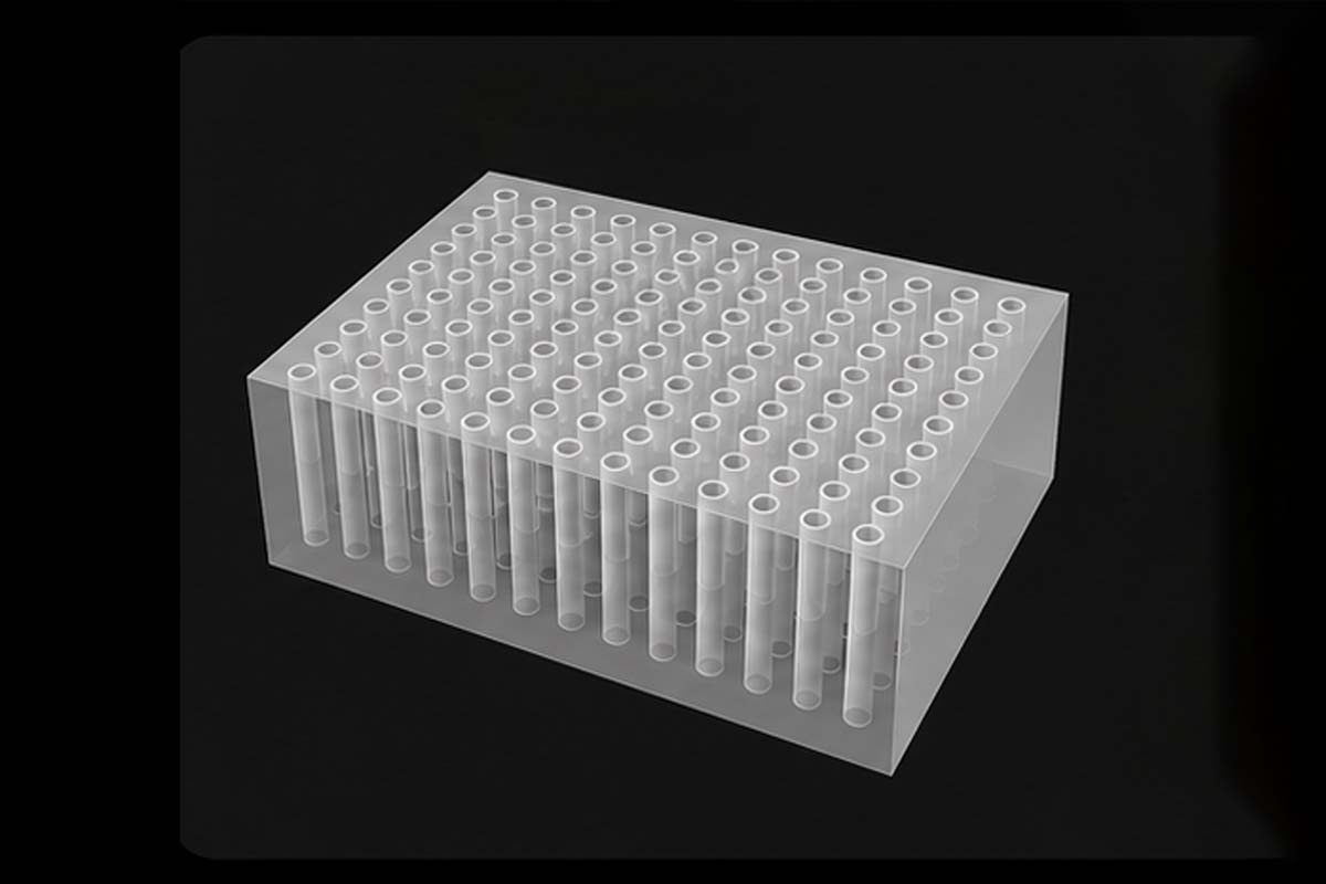
Microvia Arrays
High-density microvia arrays can be arranged across wafer or panel substrates according to the customer’s device layout and interconnect pattern.
Need Help?
Send us your via drawing, glass material, and target dimensions for a process feasibility review.
Manufacturing Capability
TGVGlass supports both wafer-level and panel-level glass microvia processing for custom TGV substrates and glass microstructures.
Substrate Options
- 2 in. to 12 in. glass wafers
- Panels up to 510 × 510 mm
- Borosilicate glass
- High-aluminosilicate glass
- Alkali-free glass
- Quartz glass
- Other technical glass materials
Structure Options
- Through holes
- Blind holes
- Oblique vias
- Waist-shaped vias
- Microvia arrays
- Custom microstructures
Process Route Options
Laser-Induced Etching
A precision route for forming small glass vias and high-density microvia patterns in TGV substrates.
Sandblasting
A flexible process for through holes, blind structures and custom glass microstructures.
Wet Etching
Available for selected glass structures where chemical material removal is suited to the required geometry.
Dry Etching
Used for selected precision microstructures requiring controlled material removal and feature definition.
Related Applications
Precision glass microvia structures for electrical, optical, sensor, display and biomedical systems.
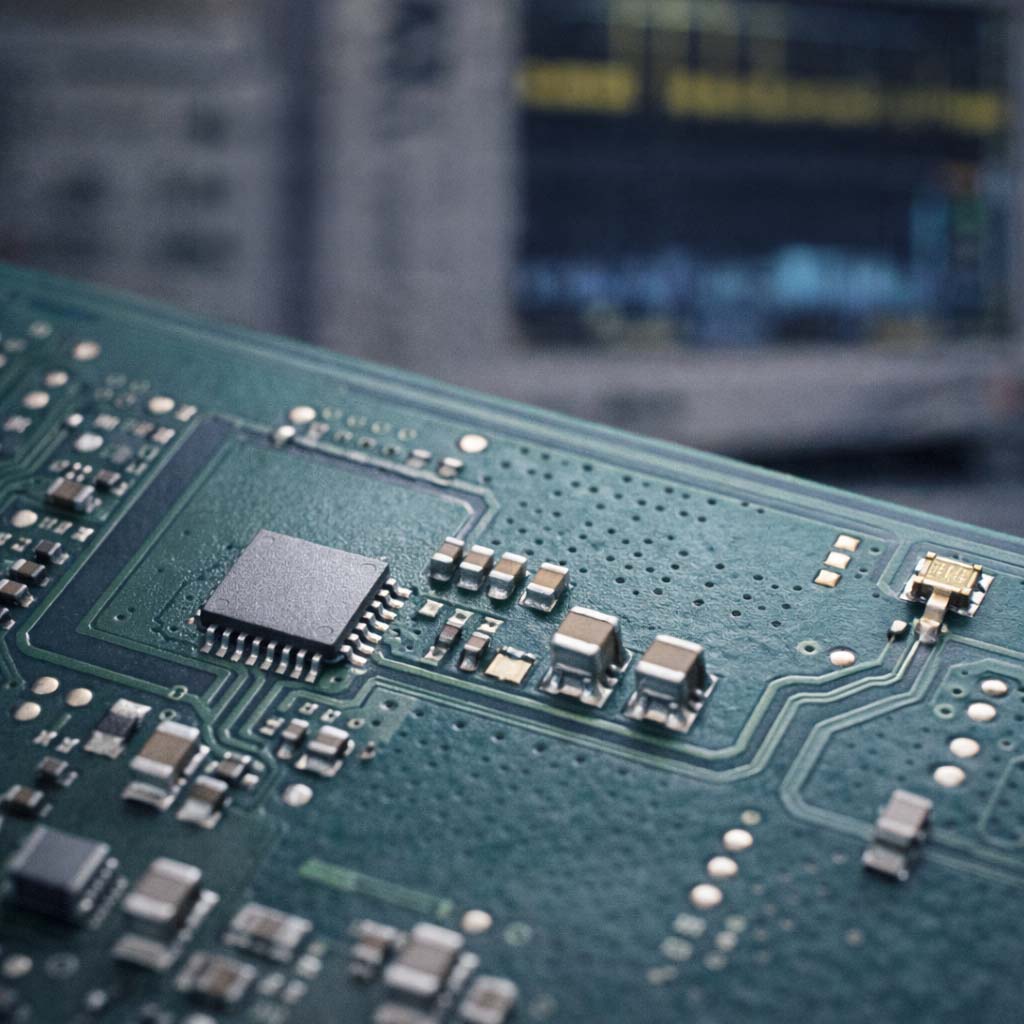
RF & High-Frequency Packaging
Glass microvias provide vertical interconnect structures for RF chips and high-frequency packaging where compact routing and high interconnect density are required.
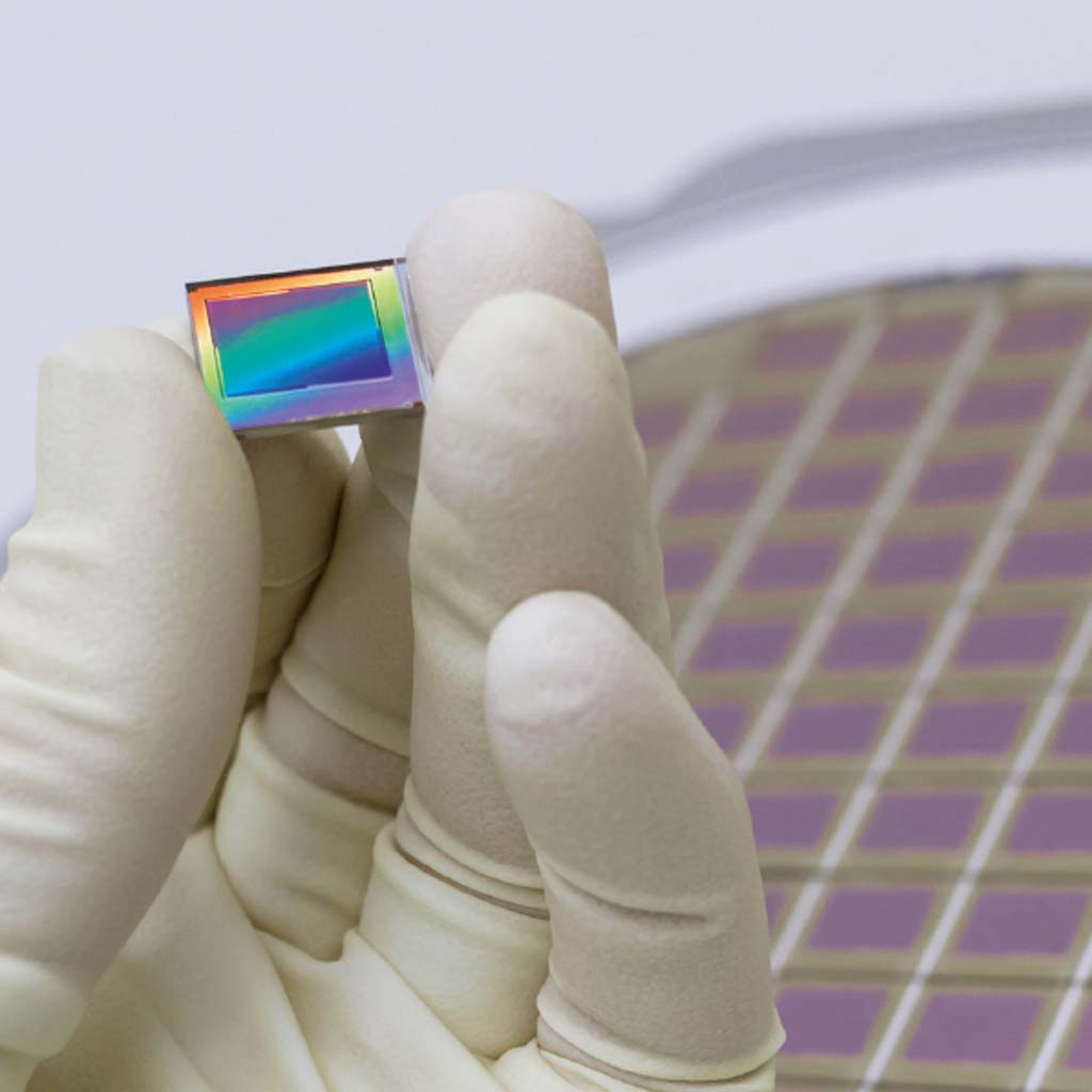
MEMS & Sensors
Through holes, blind holes and custom glass microstructures can be integrated into MEMS and sensor substrates for wafer-level packaging.
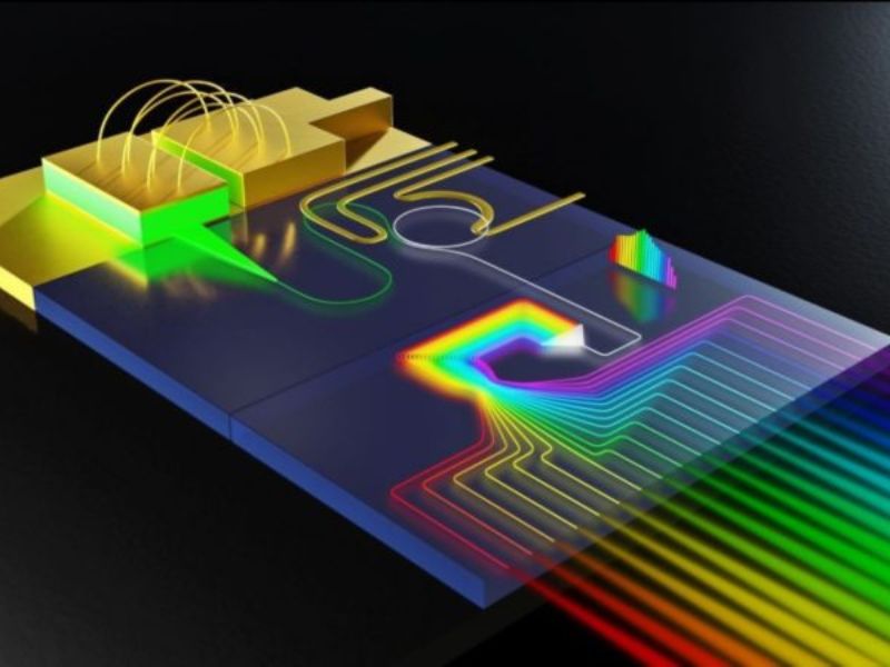
CPO & Optical Communication
Precision glass vias and microstructures can support electrical and optical integration in CPO and optical communication packaging.
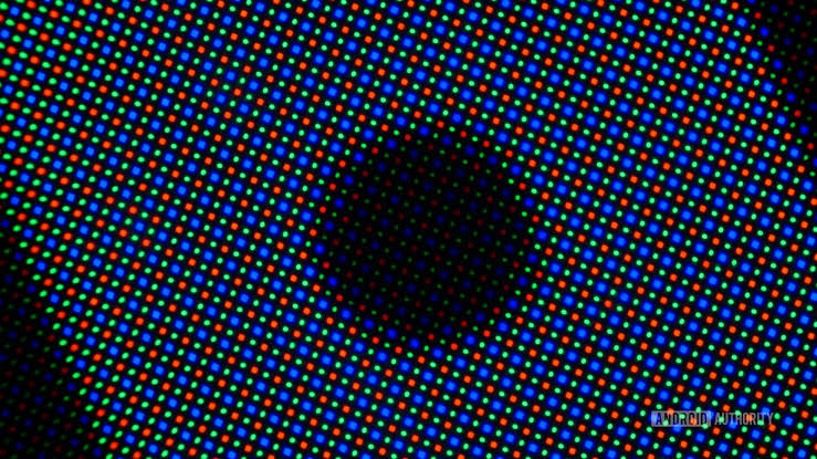
Mini-LED & Display
High-density microvia arrays can be used in display-related packaging requiring large numbers of vertical interconnect structures.
Biomedical & Microfluidic Devices
Custom glass through holes, blind holes and microstructures can also be fabricated for biomedical and microfluidic device applications.
FAQ
TGVGlass supports batch TGV microvia fabrication at diameters below 20 µm.
We support standard glass wafer formats from 2 in. to 12 in., as well as panel substrates up to 510 × 510 mm.
Yes. Blind holes are supported through our glass microstructure fabrication capability. The achievable dimensions depend on the glass material, thickness and selected process route.
Yes. Our supported structures include vertical vias, oblique vias, waist-shaped vias and custom microstructures.
Our TGV platform supports borosilicate, high-aluminosilicate, alkali-free and quartz glass, together with other technical glass materials subject to project evaluation.
The appropriate process depends on the glass material, substrate thickness, via size, geometry, density and downstream packaging requirements. Send us your drawing and our engineering team can evaluate the suitable route.
Connect with our experts
We’re here to help
Our engineers review your drawing, material, tolerances, and target quantity before quotation.
Request a Process Evaluation
Tell us about the substrate, dimensions, tolerance, quantity, processing, bonding, routing, or packaging requirements.