Manufacturing
Full-chain TGV production from glass microvia formation and filling to routing, bonding, packaging, and testing.
Markets
Custom packaging solutions for RF, MEMS, Mini-LED, AI, optics, semiconductor, communications, and sensing.
Quality
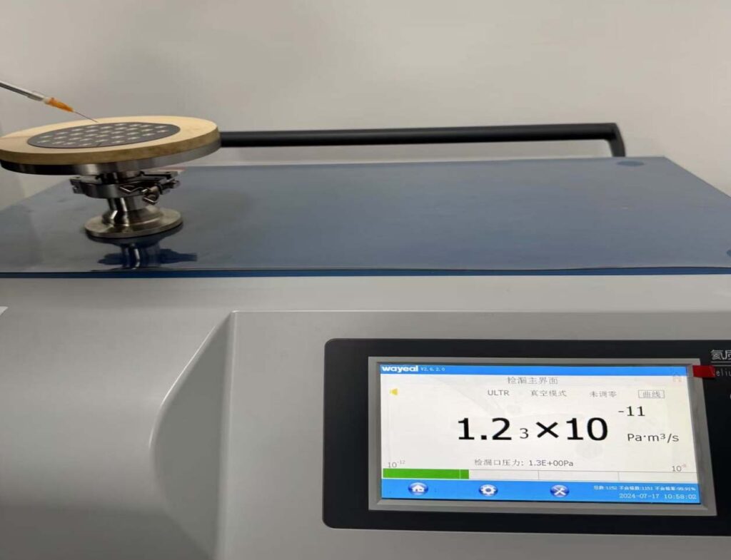
Batch microvias down to 20 µm, tolerances within ±3 µm, and hermetic leak rates below 1×10⁻¹¹ Pa·m³/s.
Research & Academic Partners
TGVGlass maintains deep research collaborations with leading institutions, advancing glass-based packaging technology.
Our Core Process Capabilities
We offer six core TGV process services covering the full packaging chain — from microvia formation to system-level packaging — delivering custom solutions from a single source.
Need Help?
Contact us for more information about our TGV packaging capabilities or to request a process evaluation.
Why TGVGlass
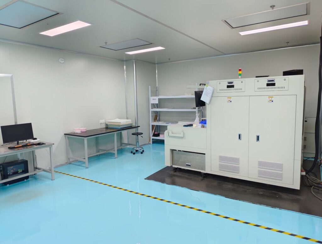
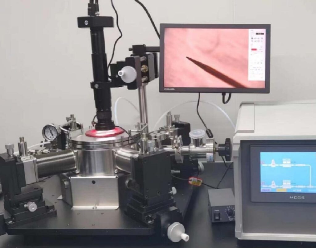
Proprietary equipment, advanced process technology, and full-chain in-house delivery.
About TGVGlass
TGVGlass is a high-tech enterprise specializing in Through Glass Via (TGV) advanced packaging technology. Equipped with advanced packaging systems and a comprehensive process flow, we deliver core capabilities across glass microvia formation, microvia metal filling, glass microstructure fabrication, wafer bonding, and multilayer RDL routing.
Our core team consists of experienced high-tech engineers with deep expertise in glass-based 3D packaging. Our packaged products are widely used across optics, semiconductor, biomedical, and communications applications.
Learn More About UsFeatured product
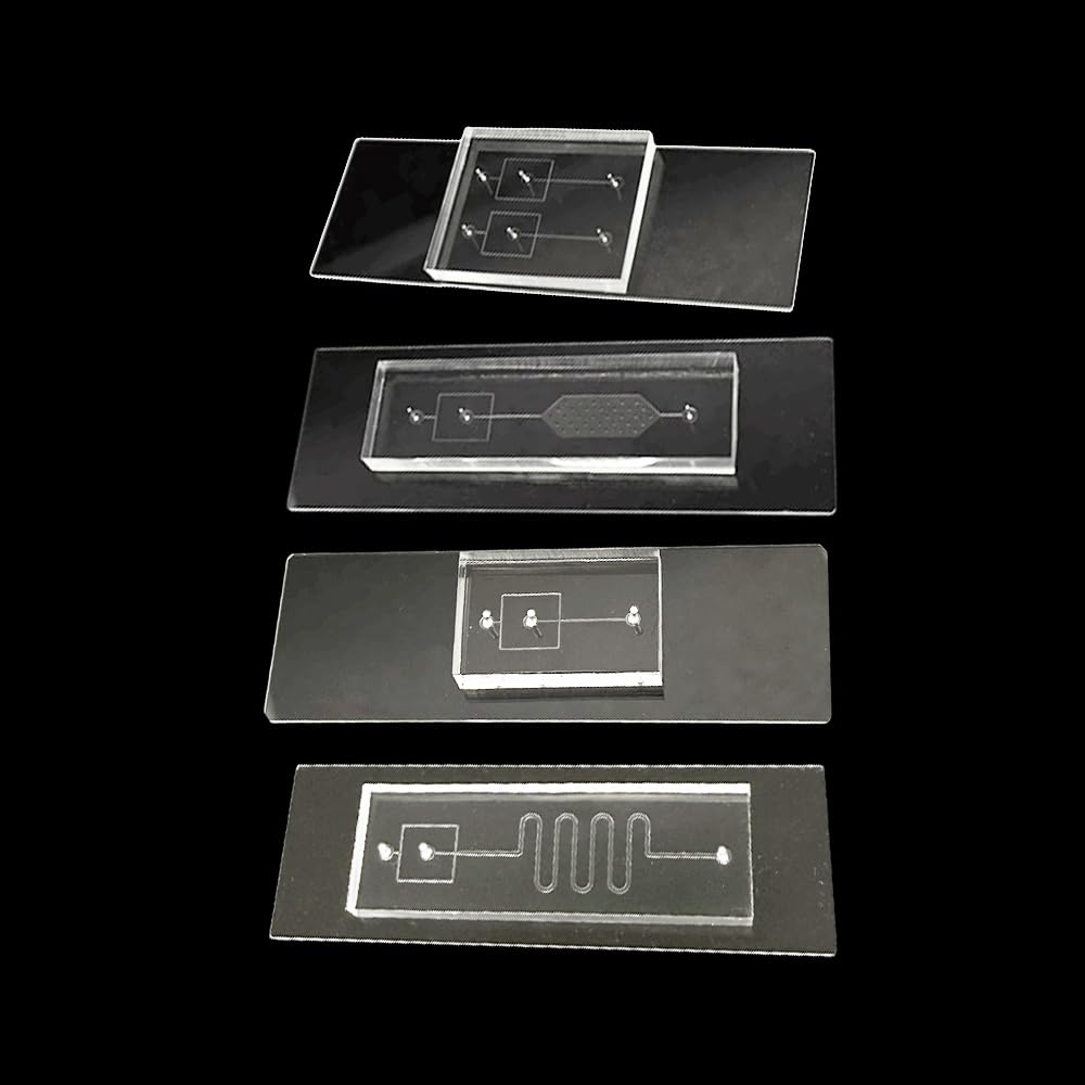
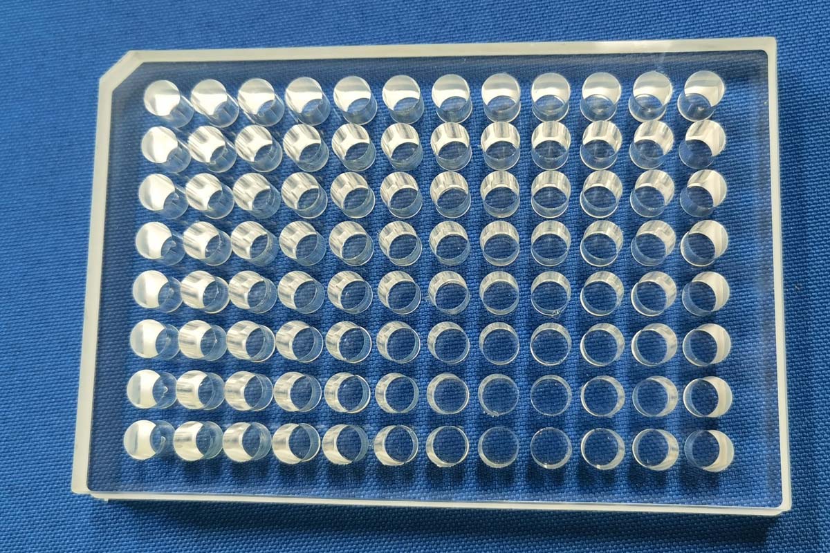
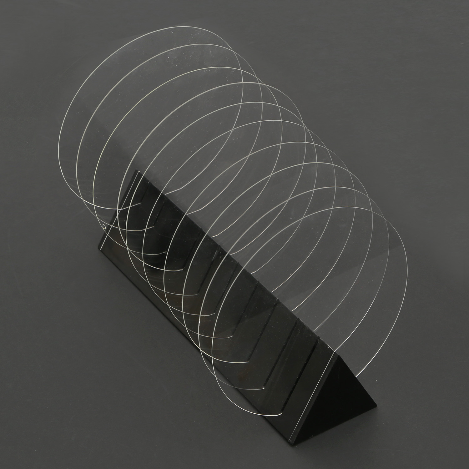
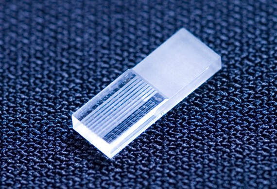
Precision glass products configured for semiconductor, MEMS, photonics, biological, and advanced packaging applications.
Technology Confidence
Built around process innovation, precision control, and close engineer-to-engineer collaboration.
Industries Served
TGVGlass’s TGV packaging technology serves a broad range of industries and applications.
Technology Insights
Process knowledge for glass interposers, high-density metallization, bonding, and system packaging.
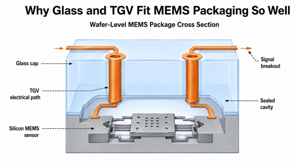
How TGV Enables High-Density MEMS and Sensor Packaging
Learn how Through Glass Via substrates support high-density MEMS and sensor packaging with compact routing, electrical isolation and wafer-level integration.
Read More »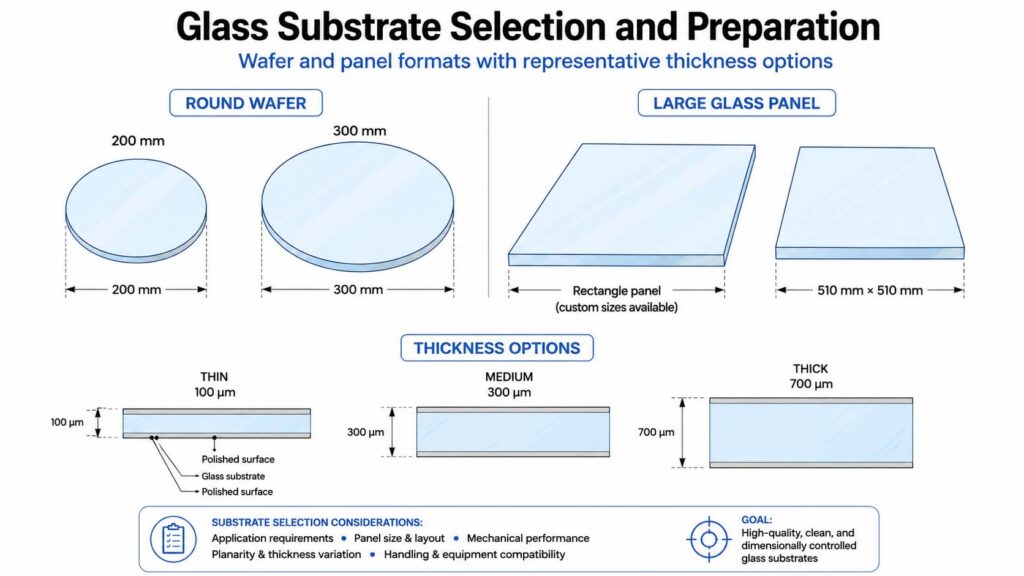
A Guide to TGV Manufacturing: From Via Drilling to Metallization
Follow the TGV manufacturing flow from glass via drilling and conditioning through seed layers, copper metallization, planarization and inspection.
Read More »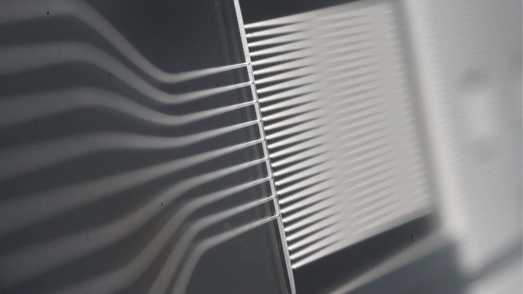
Through Glass Via for Photonic and Optical Interposers
Explore how Through Glass Via interposers enable photonic packaging, optical alignment, low-loss signal routing and compact optical-electronic integration.
Read More »Full-Chain In-House Delivery
Every process step runs on our own production line — no multi-vendor coordination required.
Process Evaluation
Review substrate, thickness, via profile, pitch, electrical requirements, thermal targets, and package integration.
Microvia & Microstructure Fabrication
Select wafer-level sandblasting or laser-induced etching, then form vias, grooves, cavities, and custom patterns.
Metallization & RDL
Apply the selected via filling route and construct multilayer redistribution routing for dense vertical interconnection.
Bonding, Packaging & Testing
Complete wafer bonding, system packaging, hermeticity evaluation, electrical inspection, and performance testing.
FAQs
Common questions about TGV manufacturing and glass-based packaging.
Connect with our experts
We’re here to help
Our engineers review your drawing, material, tolerances, and target quantity before quotation.
Request a Process Evaluation
Tell us about the substrate, via size, quantity, metallization, routing, bonding, or packaging requirements for your project.