Most TGV applications route electrical signals. Photonic interposers ask glass to do something more: carry electrical interconnects and optical signals on the very same substrate. Because glass is already an established optical material — capable of guiding light through waveguides with very low loss — combining TGVs with glass waveguides turns a single piece of glass into a platform that handles both jobs at once. This guide looks at how that combination works, why glass is uniquely positioned for it, and what’s driving its adoption in co-packaged optics.
Key Takeaways
- A photonic (or optical) interposer combines through-glass vias for electrical routing with optical waveguides built directly into the same glass substrate, connecting electronic and photonic chips in a single package.
- Glass’s dual nature — a good electrical insulator and a proven optical medium — is what makes this combination possible in a way that silicon, which needs added structures for optical routing, cannot match as directly.
- Waveguides in glass are typically formed by ion-exchange processing or by femtosecond laser direct writing, both of which have demonstrated propagation losses well under 0.3 dB/cm.
- TGVs in a photonic interposer do double duty: routing electrical power, ground, and high-speed signals between chips, while sometimes also providing structural features like grooves that align with the optical waveguide layer.
- Fiber-to-chip coupling in these designs generally uses either edge coupling or grating coupling, each with different tolerance, bandwidth, and manufacturing trade-offs.
- Glass holds its refractive index and physical dimensions more consistently across temperature than polymer or epoxy-based alignment materials, which matters directly for maintaining fiber alignment over a product’s operating life.
- Co-packaged optics (CPO) is the main driver behind photonic glass interposer development, aiming to move optical engines physically closer to switch and compute silicon to improve bandwidth density and power efficiency in AI data centers.
- Multiple companies — including Corning, Samtec, and specialized laser-processing suppliers — have published real, measured performance data for glass-based photonic interposers, not just simulation results.
Why Glass Is a Natural Fit for Photonic Interposers
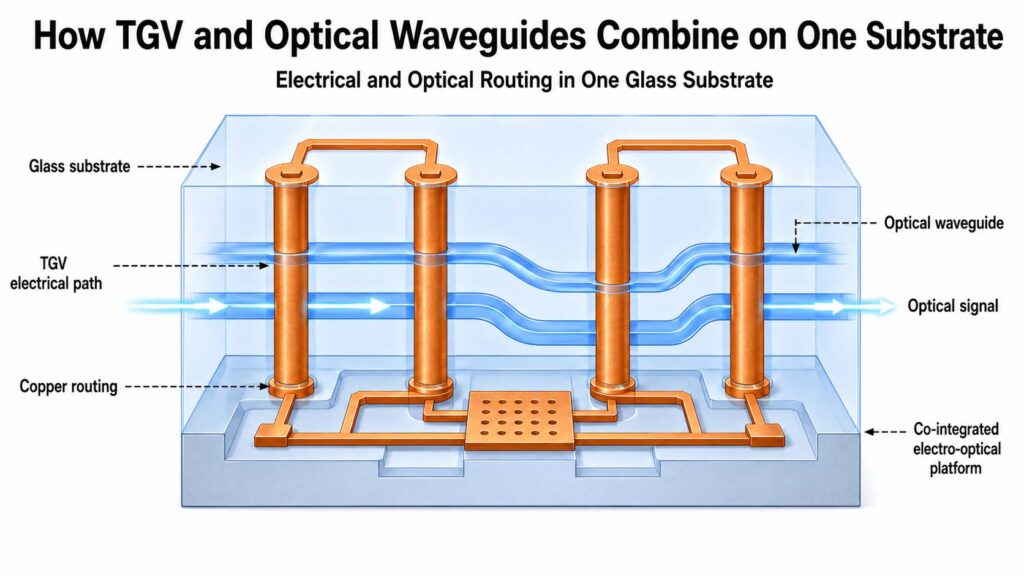
Silicon’s role in a standard TGV interposer is purely electrical — a via routes a signal, nothing more. Glass can do that same electrical job while also being the physical medium light travels through, because glass is already the material behind decades of optical fiber and waveguide technology. That dual capability means a single glass substrate can host TGVs for electrical routing and waveguides for optical routing at the same time, without bonding on a separate optical layer or routing light through free space between components.
There’s a second, less obvious advantage: glass holds its refractive index and physical geometry consistently across temperature swings that would degrade the alignment of polymer- or epoxy-based optical structures. Since fiber-to-chip and chip-to-chip optical coupling in these packages depends on alignment tolerances measured in single-digit microns, a substrate that doesn’t drift dimensionally with temperature is a real practical advantage, not just a nice-to-have. Glass also allows genuine three-dimensional waveguide routing inside the substrate volume itself, rather than being limited to surface-level routing the way silicon interposers are without additional bonding steps.
How TGV and Optical Waveguides Combine on One Substrate
Waveguide Fabrication: Ion-Exchange and Laser Writing
Two main techniques are used to put optical waveguides directly into glass. Ion-exchange (IOX) processing diffuses ions into the glass surface to locally raise the refractive index along a defined path, creating a waveguide; Corning has published work combining ion-exchange waveguides with TGVs and electrical interconnects on the same glass substrate, reporting propagation losses under 0.1 dB/cm. The alternative is femtosecond laser direct writing (sometimes called selective laser etching), where an ultrashort-pulse laser locally modifies the glass to define a waveguide path — a specialized supplier using this approach has reported propagation losses around 0.25 dB/cm along with sub-micron alignment tolerances for the associated structures. Both approaches can achieve waveguide losses well below what would meaningfully limit a data center optical link, and the choice between them tends to come down to process compatibility with the rest of the substrate’s fabrication flow rather than a large performance gap.
The Role of TGV in a Photonic Interposer
In these designs, TGVs handle the electrical side of the package the same way they do in any other TGV interposer — power delivery, grounding, and high-speed electrical signal routing between the electronic IC (EIC) and photonic IC (PIC), plus fan-out from the chips’ fine bump pitch to the coarser pitch of the board below. What’s specific to photonic interposers is that TGV geometry sometimes has to coordinate with the optical layer’s requirements as well as its own: published designs have used TGV arrays with pitches around 150 µm and opening widths under 100 µm in glass roughly 0.6 mm thick, dimensions chosen partly to leave room for the optical waveguide and coupling structures sharing the same substrate. In some architectures, precisely dimensioned grooves are cut into the glass to match the vertical distance between a flip-chip-mounted PIC’s waveguide layer and the interposer surface, so the electrical and optical fan-out geometries have to be co-designed rather than treated as separate problems.
Coupling Light In and Out
Edge Coupling vs. Grating Coupling
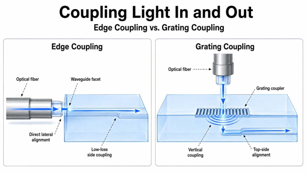
Getting light from an external fiber into an on-chip or on-substrate waveguide uses one of two general approaches. Edge coupling aligns a fiber directly with a polished edge of the chip or waveguide, often assisted by a microlens at the fiber tip to focus light into the coupler; it requires precise alignment but supports broad wavelength ranges and both polarizations. Grating coupling brings light in from above at a shallow angle, using a periodic grating structure to redirect it down into the waveguide; it tolerates looser placement precision and allows multiple rows of fibers to be used, which increases the number of optical channels per package, but grating couplers are typically more wavelength- and polarization-sensitive than edge couplers, and some designs favor one approach specifically to avoid that limitation.
Fiber Attach and Alignment Tolerance
Whichever coupling method is used, the fiber ultimately has to be mechanically attached and held in precise position relative to the waveguide, often using fiber array units (FAUs) to manage multiple fibers at once. Published designs report tight tolerances as standard: alignment accuracy in the range of ±1 µm laterally and ±2 µm vertically, with per-facet coupling losses as low as roughly 0.15-0.85 dB depending on the specific coupling scheme and how much of that loss comes from connector versus waveguide versus alignment error. These numbers matter because total link loss budget in a CPO system is tight — every fraction of a decibel lost at the fiber interface has to be made up elsewhere in the optical or electrical link.
Co-Packaged Optics: Why This Matters Now
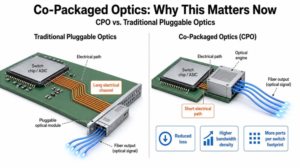
The demand pulling TGV-based photonic interposers forward is co-packaged optics (CPO) — an architecture that places optical engines physically next to (or within the same package as) a switch ASIC or compute chip, rather than relying on pluggable optical modules connected by a longer electrical trace. Moving the optics closer shortens the electrical path between the ASIC and the point where the signal converts to light, which reduces power consumption and electrical loss at the data rates modern data center switches and AI accelerators now require. CPO systems today are being built and discussed in the range of 800 Gbps to 1.6 Tbps per module, with some published switch designs demonstrating aggregate capacities in the tens of terabits per second by combining multiple CPO units with a switch chip through 2.5D packaging.
Glass has become one of the leading platforms specifically proposed for CPO because it addresses two bottlenecks at once: the electrical interconnect problem that any advanced packaging technology needs to solve, and the optical routing and alignment problem that’s unique to photonics. A glass substrate carrying both TGVs and integrated waveguides can host EICs and PICs side by side, route power and high-speed electrical signals between them through the glass, and guide light to and from external fibers through the same piece of material — collapsing what would otherwise require multiple separately aligned components into a single, dimensionally stable platform.
Real-World Performance Benchmarks
This isn’t purely a research-stage concept — multiple organizations have published measured, not simulated, results. Corning has demonstrated glass substrates combining TGVs, ion-exchange waveguides, and fiber connectors for co-packaged optics, and has publicly discussed a “Glass Bridge” optical interconnect product targeting coupling losses under 2 dB between fiber and photonic chip, with initial designs supporting photonic chip core pitches of 30 µm or greater. Samtec has demonstrated a multi-mode optical transceiver built on a TGV interposer with redistribution layers, operating at 56 Gbps per channel. IBM’s MOTION transceiver module has validated glass substrates as a viable interposer platform for CPO using TGV and RDL processes compatible with mainstream advanced packaging. In China, a collaboration between Shenguang Valley Technology and Shanghai Jiao Tong University has produced an 8-inch TGV interposer wafer, while other domestic players have pursued glass-based optical module technology through acquisition and licensing.
Taken together, these results show the core technical pieces — low-loss glass waveguides, TGV-based electrical routing, and sub-2-dB fiber coupling — are individually well demonstrated by more than one organization, even though a fully standardized, high-volume manufacturing flow for combined electro-optical glass interposers is still maturing.
Design Considerations Specific to Photonic TGV Interposers
Designing a photonic interposer isn’t just a TGV design problem with waveguides added on top — the two systems interact in ways that pure electrical TGV design doesn’t have to consider. Via placement has to leave clear paths for waveguide routing and avoid interfering with coupling structures, which can constrain via pitch and layout more than an electronics-only design would require. Warpage becomes a more acute concern as substrate size scales, since even small dimensional shifts that would be tolerable for a purely electrical interposer can misalign an optical coupling interface enough to increase loss. And because the electrical and optical systems both have to perform correctly together, design teams increasingly rely on combined electronic-photonic co-simulation — modeling TGV electrical performance and waveguide optical performance in the same simulation environment — rather than verifying each system independently and hoping the assembled result behaves as expected.
Through-glass vias were originally developed to solve an electrical routing problem, but in photonic interposers they’ve become one half of a platform that solves an electrical and an optical routing problem at the same time, on the same piece of material. That combination is a big part of why glass, rather than silicon or organic substrates, has become the leading candidate for next-generation co-packaged optics: it’s the one substrate material that was already good at guiding light before anyone needed it to also carry a via.