Glass’s low dielectric loss is the headline reason TGV interconnects outperform silicon at high frequency — but insertion loss in a real TGV channel isn’t determined by the substrate material alone. Via transitions, stub effects, crosstalk between neighboring vias, and even the power delivery network sitting next to the signal path all shape how much signal actually survives the trip through the interposer. This guide walks through where that loss comes from, a few effects that are specific to how well glass performs (rather than in spite of it), and the design techniques used to keep insertion loss under control.
Key Takeaways
- Insertion loss (S21) measures how much signal power is lost passing through a TGV interconnect; return loss (S11) measures how much is reflected back due to impedance mismatch — both matter for signal integrity.
- Impedance discontinuities at via transitions, where a signal moves from a horizontal trace to a vertical via, are a primary source of reflections and loss, especially above 10 GHz.
- Via stubs and quarter-wave resonances create sharp, frequency-specific dips in insertion loss; avoiding these frequencies within the operating band is a standard part of TGV channel design.
- Because glass is such a low-loss substrate, its power delivery network can develop unusually sharp impedance resonance peaks, which paradoxically degrade signal insertion loss by disrupting the return current path for nearby signal vias.
- At high power and high frequency, conductor loss — not dielectric loss — tends to dominate total transmission loss in TGV interconnects.
- Glass’s low thermal conductivity means self-heating from high-power signals doesn’t dissipate as easily as it would in silicon, which can shift the substrate’s electrical properties and increase insertion loss under sustained high-power operation.
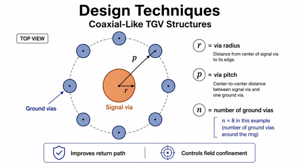
- Coaxial-like TGV structures, where a signal via is surrounded by a ring of ground vias, are a common design technique for controlling impedance and minimizing insertion loss at high frequency.
- Full-wave electromagnetic simulation, paired with S-parameter and time-domain reflectometry measurements, is the standard way to identify and correct insertion loss problems before a design is built.
What Insertion Loss and Signal Integrity Mean for a TGV Channel
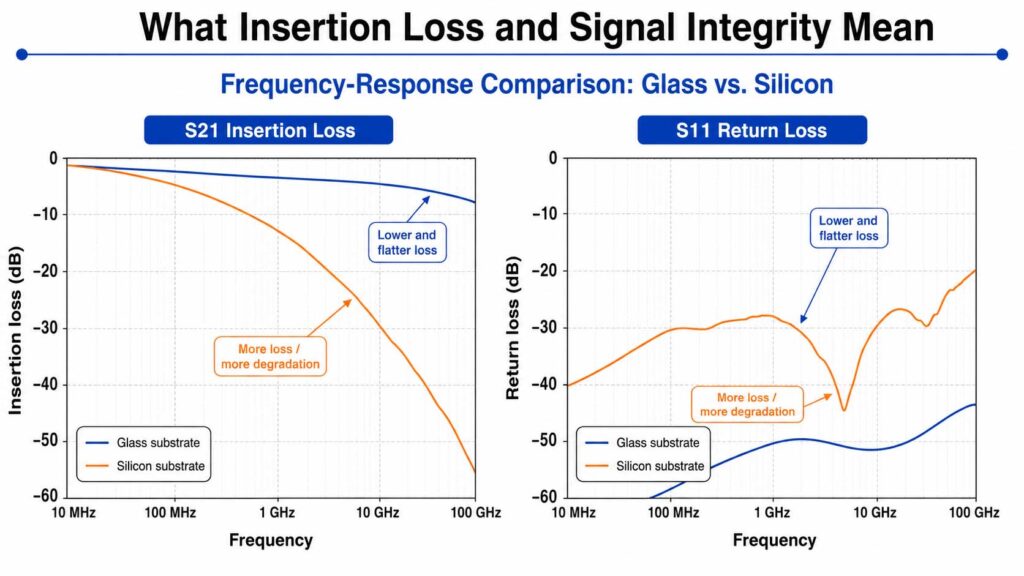
Signal integrity in a TGV interconnect comes down to two related measurements. Insertion loss (S21) describes how much of a signal’s power makes it from one end of the channel to the other — lower loss means more of the original signal arrives intact. Return loss (S11) describes how much power reflects back toward the source instead of continuing forward, which happens whenever the signal encounters a change in impedance along its path. A well-designed TGV channel keeps insertion loss low and return loss high (meaning few reflections) across the entire frequency range the signal needs to operate in, not just at a single test frequency.
Glass’s fundamental material advantage — low dielectric loss compared to silicon — gives TGV channels a real head start on this problem. Comparative measurements of microstrip lines built on glass and silicon substrates, tested up to 20 GHz, have shown substantially lower insertion loss on glass across the band, since glass’s insulating behavior doesn’t introduce the loss mechanisms that silicon’s semiconducting bulk does. But that material advantage only sets the baseline — the actual channel design still has to avoid introducing loss through geometry, discontinuities, and interactions with the rest of the package.
Where Insertion Loss Comes From in TGV Interconnects
Impedance Discontinuities at Via Transitions
The single most consistent source of trouble in a TGV channel is the transition itself — the point where a signal moves from a horizontal trace on the redistribution layer to a vertical via running through the glass, and back to a horizontal trace on the other side. Each of these transitions is a geometric discontinuity, and any discontinuity that doesn’t maintain a consistent characteristic impedance creates a reflection point. These reflections become more damaging as frequency increases; above roughly 10 GHz, even fairly small impedance variations at a via transition can meaningfully degrade signal quality.
Via Stub Effects and Quarter-Wave Resonance
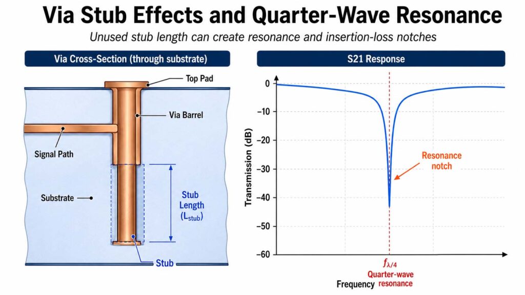
When a via runs deeper than the signal actually needs to travel — leaving an unused length of via beyond the connection point, known as a stub — that stub behaves like a small antenna, introducing excess capacitance that creates its own impedance discontinuity. This shows up as a sharp, narrow notch in the insertion loss (S21) curve at a specific resonant frequency, along with a corresponding spike in return loss (S11) at the same frequency. The underlying mechanism is quarter-wave resonance: at the frequency where the stub’s electrical length corresponds to a quarter wavelength, the mismatch is most severe, and loss increases dramatically at that frequency and its harmonics. Design teams need to identify where these resonance frequencies fall and make sure they don’t coincide with the channel’s actual operating frequency — a problem that gets more pressing as data rates rise and push operating frequencies closer to where stub resonances tend to occur.
Crosstalk Between Adjacent Vias
In dense via arrays, electromagnetic coupling between neighboring vias becomes a real signal integrity concern, and it gets worse as via pitch tightens — a design trade-off already covered in more detail in our guide to TGV design parameters. Glass’s dielectric constant, while much lower than silicon’s, is still higher than many organic substrate materials, so crosstalk in tightly packed TGV arrays needs deliberate management rather than being assumed away just because glass is a low-loss material.
Conductor Loss vs. Dielectric Loss at High Power
It’s tempting to assume dielectric loss dominates TGV channel loss, since that’s the property glass is best known for improving on silicon. But research specifically looking at high-power, high-frequency TGV transmission structures has found that under those conditions, transmission loss is primarily dominated by conductor loss — resistive loss in the copper itself — rather than loss in the glass. This matters for design priorities: at high power, improvements to conductor geometry, surface roughness, and plating quality often matter more for reducing insertion loss than further reducing the glass’s already-low dielectric loss.
The Power Delivery Network’s Surprising Role
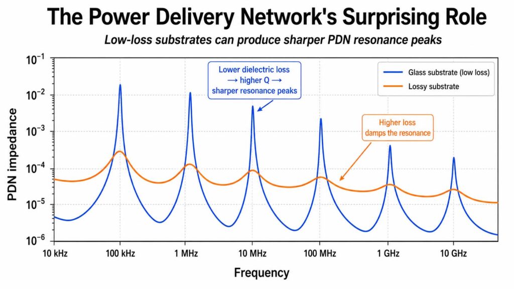
One of the more counterintuitive findings in TGV signal integrity research involves the power delivery network (PDN) — the network of power and ground vias and planes that supplies current to active circuitry, rather than the signal path itself. Because glass is such a low-loss substrate, it behaves like a high-Q (low-damping) resonant structure electrically. That’s normally a good thing, but it means the PDN built on a glass substrate can develop unusually sharp impedance peaks at its resonance frequencies — sharper than the same PDN structure would show on a lossier substrate, where resistive damping would smooth those peaks out.
At those resonance frequencies, the high PDN impedance effectively “steals” power that would otherwise support the return current for a nearby signal via, disrupting the return current path and increasing insertion loss for that signal channel — even though nothing about the signal via itself changed. In other words, glass’s low loss, which is normally the reason TGV outperforms silicon, can work against signal integrity indirectly, through the power delivery network, if PDN resonances aren’t identified and managed. This is a genuinely glass-specific effect: it’s less pronounced on lossier substrates precisely because their higher loss damps out the sharp resonance peaks that cause the problem in the first place. Practical mitigation means analyzing PDN resonance frequencies alongside signal channel design, not treating them as separate problems, and keeping those resonances away from the operating frequency band the same way stub resonances need to be avoided.
Thermal Effects on High-Power Signal Transmission
Glass’s thermal conductivity is roughly two orders of magnitude lower than silicon’s, and that gap becomes relevant for TGV interconnects carrying high-power, high-frequency signals — the kind found in high-power RF transceivers or dense high-performance computing packages. Under sustained high-power operation, self-heating from electro-thermal coupling doesn’t dissipate through low-conductivity glass as readily as it would through silicon, and that temperature rise changes the substrate’s electrical conductivity, relative dielectric constant, and loss tangent, which in turn shifts the channel’s resonance frequencies and increases insertion loss.
The effect is measurable but, in tested structures, has proven manageable within realistic power ranges: one study of TGV-connected coplanar waveguide structures under continuous-wave operation between 5 and 20 watts recorded a temperature rise of over 90°C at the highest power level, while insertion loss increased by less than half a decibel. That’s a useful data point for design margin, but it also underscores that thermal behavior needs to be evaluated specifically for high-power TGV applications rather than assumed away because glass’s electrical loss is low — electrical and thermal performance are coupled, not independent, in these structures.
Design Techniques to Minimize Insertion Loss
Impedance-Matched Via and Trace Design
The foundational technique is straightforward in principle even though it takes careful geometry in practice: designing every segment of the channel — trace, via, and the transition between them — to hold a consistent characteristic impedance, typically 50 ohms for RF applications. Demonstrated coplanar waveguide structures on glass, properly impedance-matched, have achieved insertion loss below 0.1 dB and return loss better than -20 dB at 30 GHz, showing how much headroom is available when the geometry is controlled carefully rather than left to default via and trace dimensions.
Coaxial-Like TGV Structures
For high-frequency signal vias specifically, surrounding the signal via with a ring of grounded vias — a coaxial-like structure — is a well-established technique for controlling impedance and containing the electromagnetic field close to the signal path, reducing both radiation loss and crosstalk to neighboring structures. Research optimizing this approach has modeled insertion loss as a function of via pitch, via radius, and the number of ground vias in the surrounding ring, using electromagnetic simulation combined with optimization methods to find geometries that minimize S21 loss for a target frequency — a more systematic version of the same design logic covered at a higher level in our guide to TGV design parameters.
Avoiding Stub and Resonance Effects
Where possible, minimizing or eliminating via stubs — for example, by controlling via depth so it matches the actual signal routing depth rather than running the full substrate thickness unnecessarily — removes the excess capacitance that causes stub resonance in the first place. Where a stub can’t be avoided, the design process shifts to identifying its resonant frequency through simulation and making sure that frequency falls safely outside the channel’s operating bandwidth, the same general strategy used for managing PDN resonance.
Simulation and Measurement Verification
Full-wave electromagnetic simulation is the standard tool for predicting insertion loss, return loss, and resonance behavior before a design is fabricated, letting designers iterate on via geometry, ground via placement, and stub length without building physical test structures for every variation. Once fabricated, S-parameter measurement (S11 for reflections, S21 for insertion loss) and time-domain reflectometry — which shows both the size and physical location of an impedance discontinuity along the channel — are the standard ways to verify that a design performs as simulated and to pinpoint the source of any unexpected loss.
How TGV Compares in Practice
The real-world performance numbers back up why TGV is taken seriously for RF and high-speed applications when these design principles are followed. Beyond the low insertion loss and return loss figures achievable with well-matched CPW structures, TGV-based passive components have demonstrated genuinely high quality factors — TGV inductors with Q greater than 80 (for a 3 nH inductor at 1 GHz) and integrated TGV-based metal-insulator-metal capacitors with Q greater than 560 (for 10 pF at 2 GHz) have both been reported in published work. These aren’t just interconnect numbers; they show that glass’s low-loss properties extend to on-substrate passive components built directly into the TGV structure, not just to the signal traces routed across it.
None of this happens automatically just because glass has a lower dielectric loss tangent than silicon. Insertion loss in a real TGV channel is the sum of several effects — via transition discontinuities, stub resonance, crosstalk, conductor loss, and even PDN interactions unique to how well glass performs — and managing all of them is what turns glass’s material advantage into an actual signal integrity advantage in a finished package. The channels that achieve the sub-0.1 dB losses and high-Q passives described above got there through deliberate impedance control and resonance management, not from the substrate alone.