Turning a bare sheet of glass into a working through-glass-via (TGV) substrate takes more than just drilling a hole. The via has to be formed without cracking a brittle material, coated with a conductive seed layer that reaches every wall of a high-aspect-ratio channel, filled or lined with copper, and finally connected to the rest of the package through a redistribution layer. This guide walks through that full process, step by step, from choosing the glass to the final bonded and singulated substrate.
Key Takeaways
- TGV manufacturing has two main stages — via formation and via metallization — followed by redistribution layer (RDL) build-up and final bonding or bumping.
- Via formation methods include laser drilling, laser-induced deep etching (LIDE), photosensitive glass patterning, and electrochemical or abrasive methods, each suited to different via geometries and glass types.
- Metallization starts with a thin seed layer (commonly Ti/Cu or Cr/Cu, deposited by sputtering or electroless plating) before copper is electroplated either as a conformal coating or as a complete, void-free fill.
- Conformal plating is faster and sufficient for many RF and passive-device structures; void-free fill is needed where the via itself must carry structural or high-current loads.
- Chemical mechanical planarization (CMP) flattens the surface after plating and prepares it for the redistribution layer that routes signals on and off the glass.
- Glass’s brittleness makes crack control, seed layer continuity, and void-free fill the three process areas that most determine yield.
- Common substrate materials are borosilicate glass and fused silica, chosen for their electrical, thermal, and mechanical properties.
- Panel-format processing — rectangular sheets rather than round wafers — is increasingly used to raise the usable area per production run.
Glass Substrate Selection and Preparation
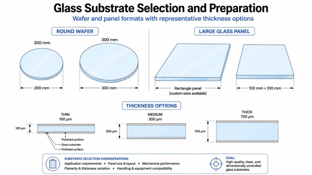
Before any via is formed, the glass itself has to be chosen and prepared. Borosilicate glass and fused silica are the two most common substrate materials, selected for their combination of electrical insulation, thermal stability, and compatibility with the via-formation method being used. Some processes use standard glass and pattern it directly with a laser or mechanical method; others use photosensitive glass, a specially formulated material that changes structure when exposed to UV light, which allows via patterns to be defined optically before etching.
Glass is available both as round wafers, sized to match standard semiconductor fab equipment, and as large rectangular panels — some suppliers process panels several hundred millimeters on a side, well beyond a standard wafer’s footprint. Panel thickness is chosen based on the application: thinner glass (well under 100 µm in some processes) suits compact, high-density packages, while thicker glass better serves applications like MEMS caps or structural interposers that need more mechanical rigidity. Handling gets progressively more delicate as glass gets thinner, since a thin, large panel has very little tolerance for the mechanical stress of transport and processing.
Via Formation: Drilling and Etching Methods
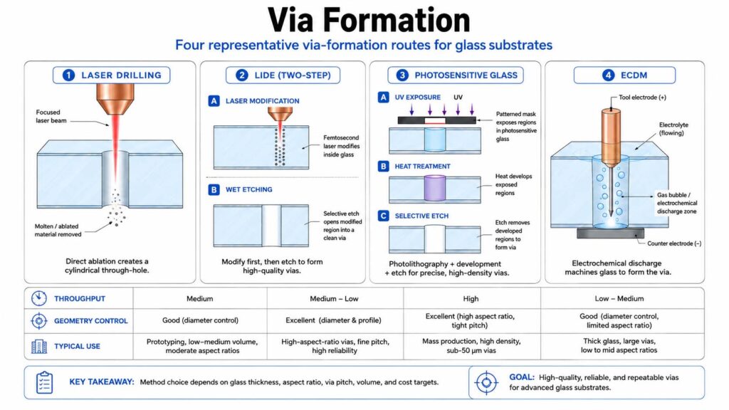
Because glass has no plastic deformation range, forming a via means removing or modifying material without introducing the cracks or micro-fractures that would compromise the substrate later. Several methods have matured for this step, each with its own trade-offs.
Laser Drilling and Ablation
Direct laser drilling uses a focused laser to ablate material and cut a hole straight through the glass. It’s flexible and doesn’t require a mask, which makes it useful for prototyping and moderate-volume production, but it can generate debris on the laser-entry side and needs careful process control to avoid micro-cracking around the via opening.
Laser-Induced Deep Etching (LIDE)
LIDE separates the “cutting” and “removing” steps. First, an ultrashort-pulse laser is focused into the bulk of the glass and scanned along the intended via path, modifying the glass’s internal structure along a narrow track — often just a few microns wide — without ablating material or introducing cracks. The panel is then immersed in a chemical etchant, such as hydrofluoric acid or a hot alkaline solution, which etches the modified glass dramatically faster than the surrounding unmodified material. Because many vias can be laser-modified in one pass and then etched together in a single bath, LIDE is well suited to high-volume, high-via-count panels.
Photosensitive Glass Patterning
In photosensitive glass, a photomask and UV exposure create a latent image of the via pattern inside the glass. A subsequent heat treatment crystallizes the exposed regions, which then etch away far faster than the surrounding glass during a wet etch step — similar in spirit to LIDE, but using light exposure through a mask instead of a scanned laser. This method can pattern a large number of vias simultaneously and doesn’t require a laser system, though it depends on a glass formulation specifically designed for photosensitivity.
Electrochemical Discharge Machining and Abrasive Methods
Electrochemical discharge machining (ECDM) and abrasive jet micromachining use localized electrical discharge or abrasive particle streams to remove glass material. These methods are generally used for larger via sizes or specific glass compositions where laser and photosensitive methods are less practical, and some lithography-free variants of ECDM can pattern both the via and the surface redistribution lines in the same step, which is useful for lower-infrastructure or research settings.
Via Metallization: Turning a Hole into a Conductor
A formed via is still just a hole in an insulator. Metallization is what turns it into a working electrical connection, and it’s arguably the step where TGV process yield is won or lost.
Seed Layer Deposition
The first metallization step deposits a thin, continuous conductive layer on the via walls to serve as the foundation for electroplating. This is typically a titanium-copper or chromium-copper stack — the titanium or chromium acts as an adhesion layer between the glass and the copper — applied by sputtering or evaporation. Electroless plating is a common alternative, particularly for high-aspect-ratio vias where line-of-sight sputtering struggles to coat the full depth of the via wall; electroless processes typically use a catalytic activation step (often a palladium-based catalyst) followed by chemical deposition of nickel or copper, building up a seed layer roughly a few hundred nanometers thick. Whichever method is used, seed layer continuity is critical: any gap in coverage — especially near the bottom of a deep via — becomes a starting point for voids in the copper fill that follows.
Copper Electroplating: Conformal vs. Void-Free Fill
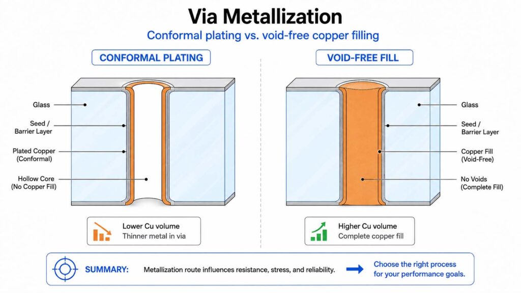
Once the seed layer is in place, copper is electroplated onto it, and the process branches into two general approaches depending on what the via needs to do electrically and mechanically:
- Conformal plating coats the via walls with a controlled thickness of copper — often in the range of a few to around fifteen microns — without fully filling the via. This is faster than a complete fill and is often sufficient for RF structures like integrated inductors, where the goal is a low-resistance conductive path rather than a solid metal plug.
- Void-free (bottom-up) fill completely fills the via with copper, which gives lower overall resistance and better mechanical and thermal performance, at the cost of a longer, more carefully controlled plating process. Bottom-up filling relies on plating bath additives that suppress deposition at the via opening while accelerating it at the via bottom, so the via fills progressively from the bottom rather than pinching closed at the top and trapping a void inside.
Both approaches depend on plating bath chemistry and current control to manage deposition rate evenly across a panel; without that control, high-aspect-ratio vias are especially prone to voids, and low-aspect-ratio or shallow features can plate unevenly across a large panel.
Chemical Mechanical Planarization (CMP)
After plating, the panel surface is polished flat by chemical mechanical planarization, which removes the excess copper that was deposited across the field area (not just inside the vias) and leaves a smooth, flat surface with the via tops exposed. This step is what makes the surface ready for the redistribution layer that follows — any residual copper or surface irregularity at this stage can cause alignment or adhesion problems downstream.
Redistribution Layer (RDL) and Back-End Integration
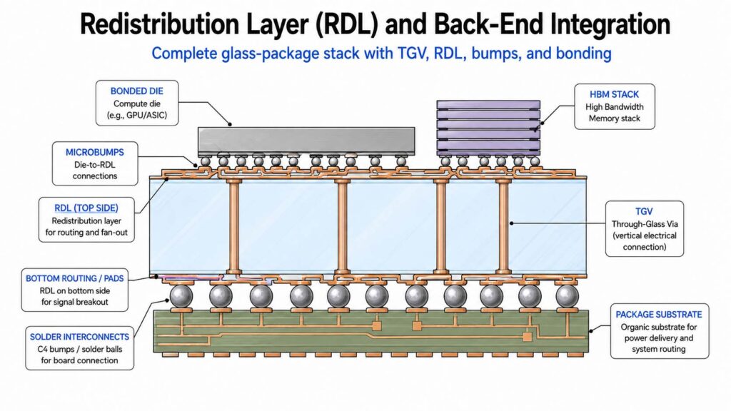
Building the RDL
With the vias formed and metallized, the substrate still needs circuitry connecting those via locations to the pads and traces where dies or bumps will eventually attach. The redistribution layer is built using photolithography to pattern a resist layer, followed by metal deposition and etching (or, in additive processes, plating directly into the patterned openings) to create the interconnect traces on one or both sides of the glass. RDL formation is highly sensitive to alignment with the underlying vias — a misregistered RDL layer can create open circuits or unwanted shorts — and to the cleanliness of the surface it’s built on, since residual ionic contamination can affect long-term reliability even if the substrate passes initial electrical testing.
Bonding, Bumping, and Singulation
Depending on the application, a finished TGV substrate may be anodically bonded to a silicon wafer (common in MEMS capping, where a hermetic seal is required), fitted with under-bump metallurgy and solder bumps for flip-chip attachment, or laminated into a larger package as an interposer. The final step is singulation — typically laser dicing — to separate individual devices or interposers from the processed panel.
Process Control and Yield Considerations
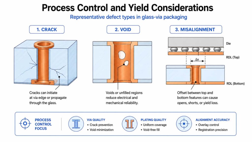
Every step in this process is a place where a brittle, insulating material can go wrong in ways that a more forgiving substrate like silicon or organic laminate would not. Micro-cracks introduced during via formation can propagate during later thermal or mechanical processing. Incomplete seed layer coverage — especially at the bottom of a high-aspect-ratio via — leads directly to voids during copper fill, which show up as resistance variation or reliability failures later. Misaligned RDL patterning can turn an otherwise good via into a defective circuit. And because TGV processing is increasingly moving toward large rectangular panels to capture cost advantages, defect density has to be controlled across a much larger area than a single round wafer, or the yield benefit of panel-scale processing can be offset by scrapping larger and more expensive pieces of material when something goes wrong.
In practice, this means TGV manufacturing lines invest heavily in inspection between steps — checking via geometry and cleanliness after formation, seed layer continuity before plating, and fill quality (often by X-ray or cross-sectional imaging) before committing a panel to RDL build-up. Some suppliers report via yields above 95% on mature processes, though the achievable yield on any given line depends on via density, aspect ratio, and panel size, so it’s worth treating any single reported number as a data point rather than an industry-wide standard.
Getting from a bare glass panel to a finished TGV substrate is a sequence of steps that each have to work correctly for the final part to work at all: forming a clean via without cracking the glass, building a continuous seed layer inside it, filling or lining it with copper without trapping voids, planarizing the surface, and then routing signals across it with a well-aligned redistribution layer. None of these steps is exotic on its own — laser processing, electroplating, and photolithography are all mature techniques elsewhere in electronics manufacturing — but doing all of them reliably on a brittle, insulating substrate, at increasing panel scale, is what separates a TGV process that works in the lab from one that’s ready for high-volume production.
FAQ
What are the two main stages of TGV manufacturing? Via formation (creating the hole through the glass) and via metallization (making that hole electrically conductive), followed by redistribution layer build-up and final bonding, bumping, or singulation.
What’s the difference between LIDE and direct laser drilling? Direct laser drilling ablates material to cut the via in one step. LIDE separates the process into two steps: a laser first modifies the glass’s internal structure without removing material, and a chemical etch then dissolves the modified glass much faster than the surrounding material, producing a cleaner via with less risk of cracking.
Why does the seed layer matter so much for TGV reliability? The seed layer is what makes the via wall conductive enough for electroplating to work. Any gap in seed layer coverage — which is more likely in deep, high-aspect-ratio vias — becomes a starting point for voids in the copper fill, which can cause resistance variation or long-term reliability problems.
Should a TGV via be fully filled with copper or just coated? It depends on the application. Fully filled (“void-free”) vias offer lower resistance and better mechanical and thermal performance, useful for structural or high-current paths. Conformal plating, which coats the walls without a full fill, is faster and often sufficient for RF structures like integrated inductors.
What is CMP used for in TGV manufacturing? Chemical mechanical planarization polishes the panel surface flat after copper plating, removing excess copper from the field area and creating a smooth surface with the via tops exposed — a necessary step before building the redistribution layer.
What is the redistribution layer (RDL) and why is alignment so important? The RDL is the patterned metal circuitry built on the glass surface that connects the via locations to the pads, traces, and bump sites used to attach dies or connect to the next level of packaging. Because it has to line up precisely with the vias underneath it, misalignment can create open circuits or shorts.
What materials are commonly used for TGV substrates? Borosilicate glass and fused silica are the most common, chosen for their electrical insulation, thermal stability, and compatibility with laser or photosensitive via-formation methods.
What causes most yield loss in TGV manufacturing? Micro-cracking during via formation, incomplete seed layer coverage in high-aspect-ratio vias, voids from incomplete copper fill, and RDL misalignment are the most common yield-limiting issues, and all of them tend to become harder to control as panel size increases.