A MEMS sensor is only as good as its package. An accelerometer, a gyroscope, and a microphone all need fundamentally different sealed environments to work correctly, and every one of them still needs an electrical connection running from the moving structure inside the cavity to the outside world without breaking the seal. Through-glass vias solve exactly that problem — routing signals through a hermetically sealed glass cap without a single wire crossing the boundary — which is why glass and TGV have become such a common pairing in wafer-level MEMS packaging. This guide looks at how that combination works and what it actually delivers in practice.
Key Takeaways
- Glass is a natural MEMS packaging material because it combines high geometrical tolerance, chemical and heat resistance, and the ability to form a reliable hermetic seal with silicon, all in one substrate.
- Anodic bonding is the dominant method for sealing a glass cap to a silicon MEMS wafer, typically performed at 350-400°C with several hundred volts applied, without needing an intermediate sealing material.
- Glass frit bonding is a common alternative, offering patternable seal geometry and good hermeticity without requiring an applied bonding voltage, and is widely used for gyroscopes, accelerometers, and RF resonators.
- TGV geometry for MEMS packaging is typically coarser than TGV used in IC interposers — vias in the range of hundreds of microns rather than tens of microns are common, since the goal is a reliable electrical feedthrough rather than dense signal routing.
- Different MEMS devices need different sealed environments: accelerometers generally need atmospheric-pressure sealing for damped response, while gyroscopes need vacuum sealing to maximize resonant sensitivity — and multi-step anodic bonding processes can seal both in a single wafer-level run.
- Vacuum packaging enabled by TGV and glass caps has been shown to improve gyroscope quality factor (Q) by roughly an order of magnitude compared to unencapsulated devices in published research.
- Commercial hermetic TGV glass wafer products, such as SCHOTT’s HermeS, are already available specifically for industrial, medical, and RF MEMS packaging applications.
- Getter materials integrated into the sealed cavity are commonly used to maintain vacuum levels over time, with published devices demonstrating stable hermeticity over periods of many months to multiple years.
Why Glass and TGV Fit MEMS Packaging So Well
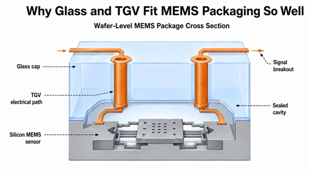
MEMS devices — accelerometers, gyroscopes, pressure sensors, microphones, RF switches and resonators — all share one requirement that sets them apart from ordinary ICs: they contain a moving or physically sensitive structure that has to be protected from the environment while still being electrically connected to the outside world. Glass addresses both halves of that problem in a single material. Its high geometrical tolerance, chemical resistance, and heat resistance make it a stable, reliable capping material, and its long history of anodic and frit bonding to silicon means the seal itself is a mature, well-characterized process rather than a novel one. TGVs then solve the electrical half: instead of routing signal wires around the sealed boundary (which would break the seal) or relying on wire bonds that add height and complexity, a TGV runs straight through the glass cap itself, providing a feedthrough that maintains hermeticity while still carrying a signal from inside the cavity to outside contacts.
This combination is also why glass fits so naturally into wafer-level packaging (WLP) for MEMS: because the cap, the seal, and the electrical feedthroughs are all formed at the wafer level before dicing, a single process run can seal and interconnect hundreds or thousands of individual sensor die at once, which is central to the cost economics of consumer-scale MEMS devices like the accelerometers and gyroscopes found in phones and wearables.
Bonding Methods for Hermetic MEMS Packaging
Anodic Bonding
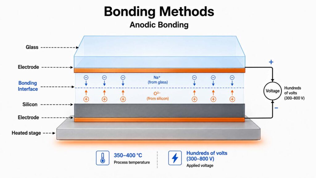
Anodic bonding is the most widely used method for sealing a glass cap directly to a silicon MEMS wafer. The process typically runs at 350-400°C with a bonding potential in the range of several hundred volts applied across the glass-silicon interface, and it doesn’t require any intermediate sealing material on either surface — the bond forms directly between the glass and silicon under the combination of heat and applied voltage. Published processes have achieved packaging yields around 94% with cavity pressures as low as roughly 1 mTorr when combined with an activated getter, and reported hermeticity as tight as 0.1 × 10⁻⁹ atm·cc/s under standard leak-test methods — tight enough to meet demanding military and industrial reliability standards.
Glass Frit Bonding
Glass frit bonding uses a patterned, screen-printed glass paste as an intermediate bonding layer rather than bonding the glass and silicon surfaces directly. Its main advantages are that the seal geometry can be precisely patterned, it doesn’t require an applied bonding voltage during the process, and — depending on the frit formulation — it can offer less CTE mismatch sensitivity than direct glass-to-silicon bonding, which matters for larger sealed cavities or where thermal cycling reliability is a priority. Glass frit bonding is widely used specifically for gyroscopes, accelerometers, and RF resonators, where a reliable hermetic seal directly affects device performance and long-term stability.
Choosing Between Methods
Other bonding approaches — eutectic bonding, direct silicon-to-silicon bonding, adhesive bonding, and transient liquid phase (TLP) bonding — each have a role in specific MEMS packaging flows, particularly where a design needs a lower bonding temperature or a specific combination of cap and device materials that anodic or frit bonding doesn’t suit well. In practice, the choice usually comes down to what pressure and hermeticity level the specific device needs, what temperature budget the rest of the wafer stack can tolerate, and whether the bonding process needs to accommodate more than one sealed pressure environment on the same wafer — a scenario covered in more detail below.
TGV Geometry and Metallization for MEMS
TGV design for MEMS packaging looks noticeably different from TGV design in a high-density IC interposer, because the job is different: a MEMS feedthrough needs to carry a handful of signals reliably through a hermetic seal, not route thousands of I/O connections at fine pitch. Published MEMS TGV processes have used via diameters in the hundreds of microns — for example, laser-ablated square vias around 300 µm through BF33 glass, or powder-blasted biconical vias around 600 µm in diameter through 500 µm glass — geometries that would be considered very coarse for an IC interposer but are entirely appropriate for a MEMS feedthrough, where mechanical robustness and reliable metallization matter more than density.
Metallization for MEMS TGVs is also often simpler than the full void-free copper fill used in IC interposers. Electron-beam evaporated metal coating the via walls, rather than a complete electroplated fill, is a common and sufficient approach for many MEMS feedthroughs, since the goal is a low-resistance electrical path rather than a structural, fully dense conductor. One notable MEMS-specific variant is the glass reflow (or glass-in-silicon, GIS) technique, where molten glass flows into holes formed in a silicon wafer via capillary action, and a low-resistance silicon pillar embedded in that glass serves simultaneously as the electrical feedthrough and, in some capacitive sensor designs, as a fixed capacitor plate — a dual-function approach that simplifies the overall device structure compared to forming a separate TGV and a separate sensing electrode.
Different Sensors, Different Sealing Requirements
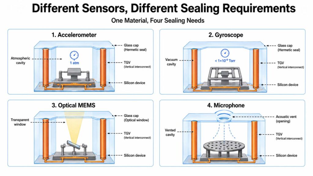
Not every MEMS device wants the same sealed environment, which is part of what makes hermetic TGV packaging genuinely useful rather than a one-size-fits-all solution. Accelerometers generally need to be sealed at or near atmospheric pressure, since their damped oscillator structure relies on air damping to achieve a fast, stable response. Gyroscopes need the opposite: they achieve high sensitivity through large resonant displacement, which air damping would suppress, so they need to be sealed in a vacuum to perform well. Optical MEMS sensors need a transparent package that doesn’t attenuate the signal they’re designed to detect — an application where glass’s own optical transparency is a direct advantage over an opaque cap material. Acoustic sensors like MEMS microphones need the opposite of a fully sealed cavity: a carefully engineered opening that lets sound pass through while still blocking dust and moisture. RF MEMS switches and resonators need a controlled, stable pressure environment because their quality factor is directly sensitive to the surrounding atmosphere.
This diversity of requirements is where multi-step anodic bonding becomes genuinely valuable: published wafer-level packaging research has demonstrated a process that seals an accelerometer at atmospheric pressure and a gyroscope in vacuum in the same wafer run, using a first bonding step performed in atmosphere followed by a pressure-control step and a second bonding step performed in vacuum. That kind of process lets a single combined inertial measurement package — accelerometer and gyroscope together, a common combination in real products — get each sensor the sealed environment it actually needs without requiring two entirely separate packaging flows.
Real Performance Gains from TGV-Based Vacuum Packaging
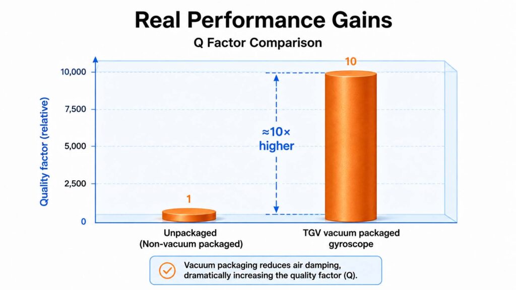
The performance benefit of getting this right isn’t theoretical. Published research on TGV-sealed capacitive gyroscopes using anodic-bonded glass caps has reported quality factors exceeding 220,000 — roughly an order of magnitude higher than the same class of device left unencapsulated. A separate study of a wafer-level sandwich-packaged butterfly vibratory gyroscope, using a glass-in-silicon composite substrate and anodic bonding, measured Q factor improvements of roughly 8.6x in drive mode and 2.8x in sense mode compared to a traditional ceramic shell package. On the reliability side, TGV-sealed gyroscope packages have been tested maintaining a vacuum of around 1 Pa for over two years, and separate glass-frit-sealed devices with integrated getters have shown stable hermeticity over 70-day test periods after initial pressure stabilization — evidence that these aren’t just clean lab demonstrations but packages that hold their sealed environment over realistic timeframes.
Commercially, this approach has moved well past the research stage: SCHOTT’s HermeS glass substrate wafer is a dedicated commercial product built specifically around hermetically sealed, solid through-glass vias for MEMS packaging, marketed for industrial hermetic MEMS sensors, medical MEMS, and RF MEMS applications, with fine-pitched vias for reliable signal and power feedthrough and glass’s inherently low dielectric constant supporting good RF performance alongside the hermetic seal.
Getting a MEMS sensor’s package right is, in a real sense, as important as getting the sensor structure itself right — a gyroscope with a poorly sealed cavity will never reach the Q factor its mechanical design is capable of, no matter how well the moving structure was fabricated. TGV-based glass packaging has become a standard answer to this problem specifically because it solves the sealing and the electrical feedthrough requirements with one material and one wafer-level process, rather than treating them as separate problems to be solved with separate materials and separate process steps.
FAQ
Why is glass commonly used for MEMS packaging caps? Glass combines high geometrical tolerance, chemical and heat resistance, and a mature, well-characterized ability to form hermetic seals with silicon through anodic or glass frit bonding — properties that make it a reliable, cost-effective capping material for wafer-level MEMS packaging.
How does anodic bonding work for MEMS sealing? Anodic bonding applies heat (typically 350-400°C) and a high voltage (often several hundred volts) across a glass-silicon interface, forming a direct bond without needing any intermediate sealing material. It’s the most widely used method for sealing glass caps to silicon MEMS wafers.
Why do accelerometers and gyroscopes need different sealed environments? Accelerometers rely on air damping in their oscillator structure to achieve a fast, stable response, so they’re typically sealed near atmospheric pressure. Gyroscopes achieve sensitivity through large resonant displacement, which air damping would suppress, so they need to be sealed in a vacuum to perform well.
Can one wafer-level process seal both an accelerometer and a gyroscope with different pressure requirements? Yes. Published research has demonstrated multi-step anodic bonding processes — bonding in atmosphere first, then a pressure-control step, then a second bonding step in vacuum — that seal an accelerometer at atmospheric pressure and a gyroscope in vacuum within the same wafer run.
How is TGV geometry different for MEMS packaging compared to IC interposers? MEMS TGVs are generally much coarser, often in the range of hundreds of microns in diameter, since the goal is a reliable electrical feedthrough for a handful of signals rather than dense high-count signal routing. IC interposer TGVs are typically tens of microns in diameter to support much higher via density.
Does TGV vacuum packaging actually improve MEMS device performance? Yes, measurably. Published research has shown TGV-sealed, vacuum-packaged gyroscopes achieving quality factors an order of magnitude higher than unencapsulated devices, and separate studies have reported several-times Q factor improvements compared to traditional ceramic shell packages.
What is a getter, and why is it used in MEMS vacuum packaging? A getter is a material integrated into the sealed cavity that absorbs residual gas molecules after sealing, helping achieve and maintain a lower internal pressure over time. Getters are commonly activated after bonding and have been shown to help sustain stable vacuum levels over many months of testing.
Are there commercial products built around TGV-based MEMS packaging? Yes. SCHOTT’s HermeS glass substrate wafer is one example — a commercially available hermetic TGV glass wafer product marketed specifically for industrial, medical, and RF MEMS packaging applications.