Microstructures We Make
Custom holes, grooves, channels, cavities and patterned structures manufactured according to the device drawing.
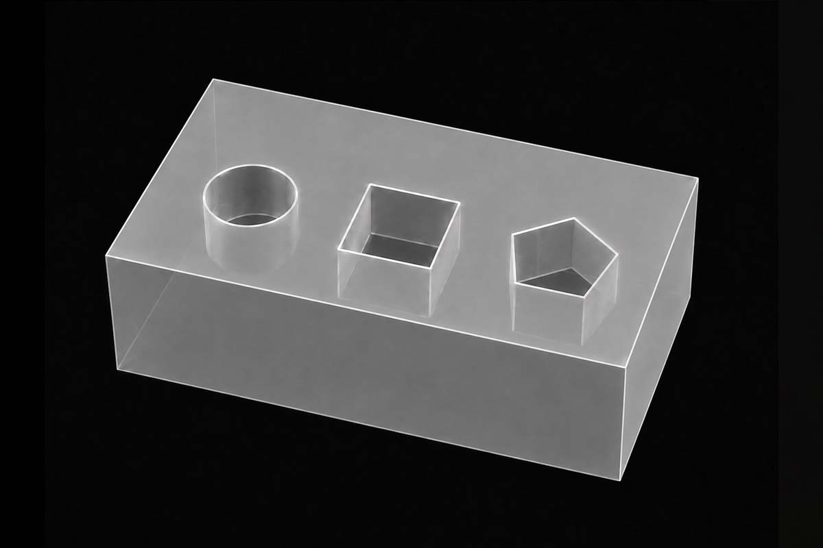
Custom-Shaped Holes
Irregular and application-specific hole geometries can be fabricated according to customer drawings and device layouts.
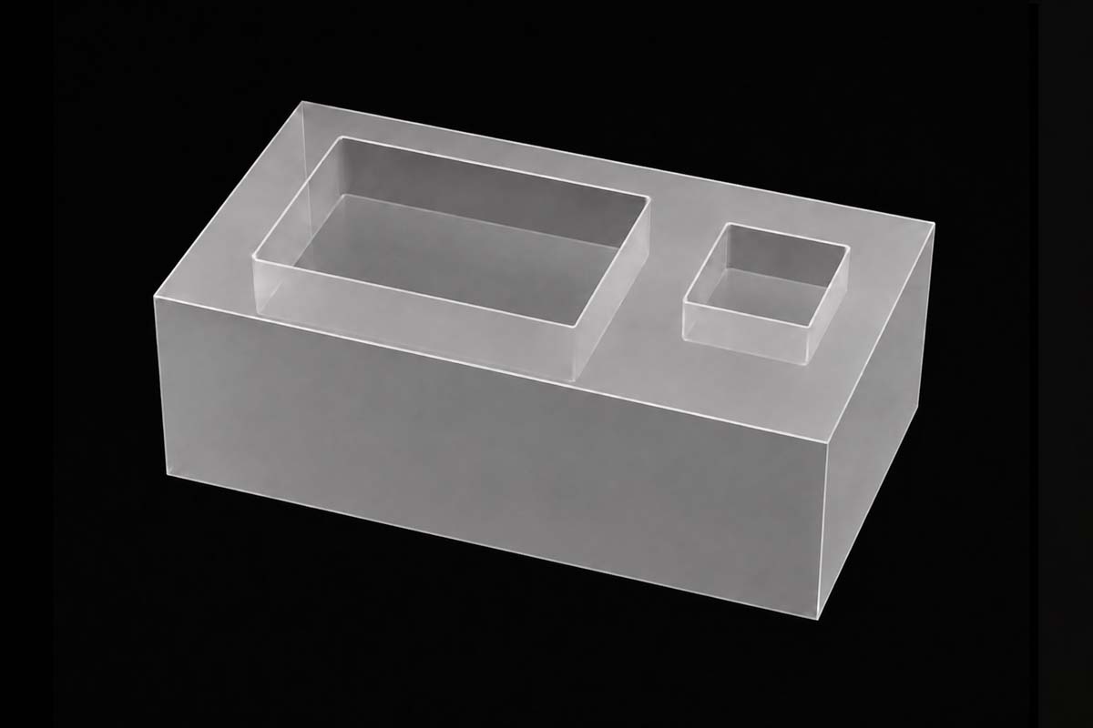
Precision Grooves
Custom grooves can be processed in glass and other technical substrates for fluidic, mechanical and packaging structures.
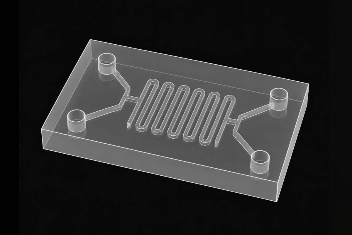
Microchannels
Precision channel structures can be fabricated for microfluidic chips, biomedical devices and other microsystem applications.
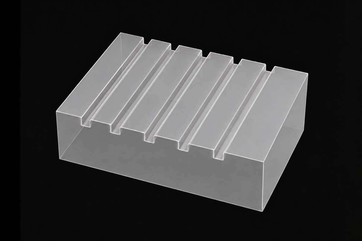
Cavities
Custom recessed and cavity structures are available for devices requiring local depth control, component clearance or packaging space.
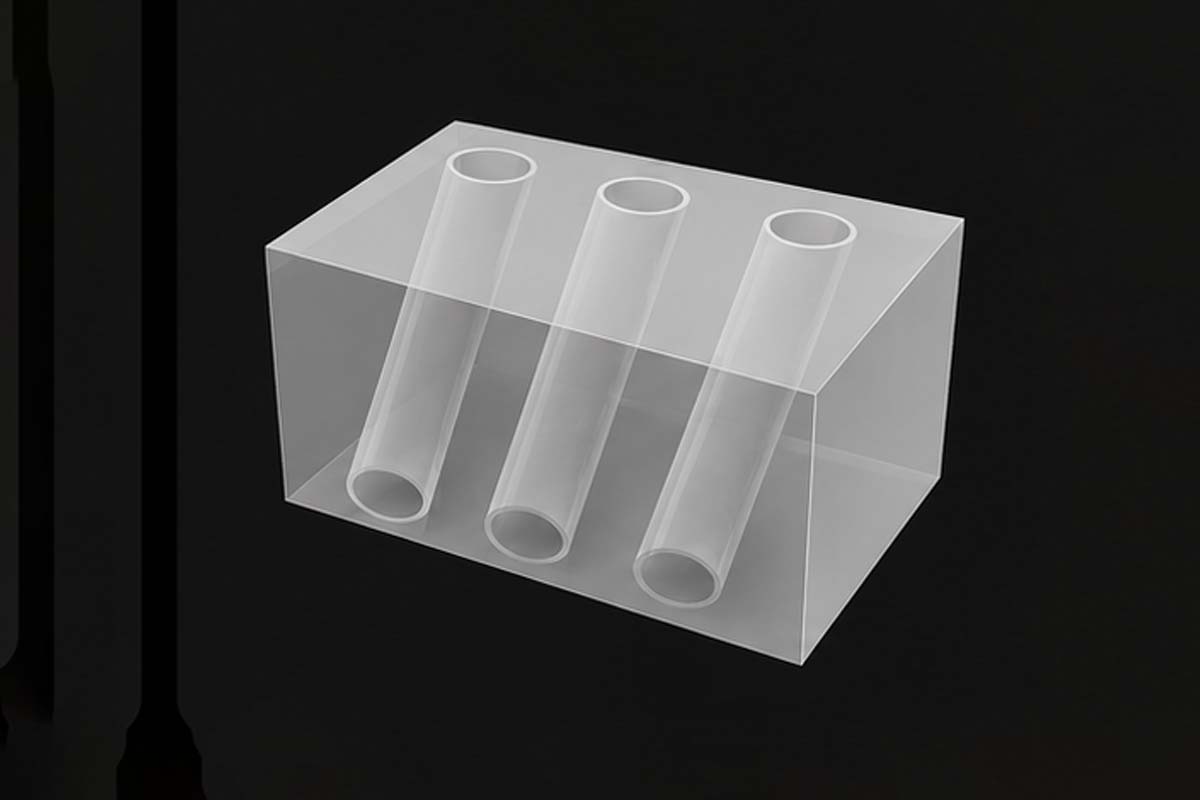
Oblique Holes
Angled holes can be fabricated where vertical structures cannot meet the required device or interconnect geometry.
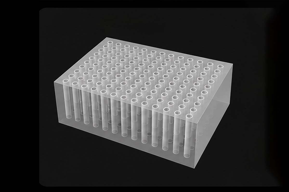
Fiber Insertion Holes
Precision glass microholes can be used for fiber insertion and positioning in optical and photonic assemblies.
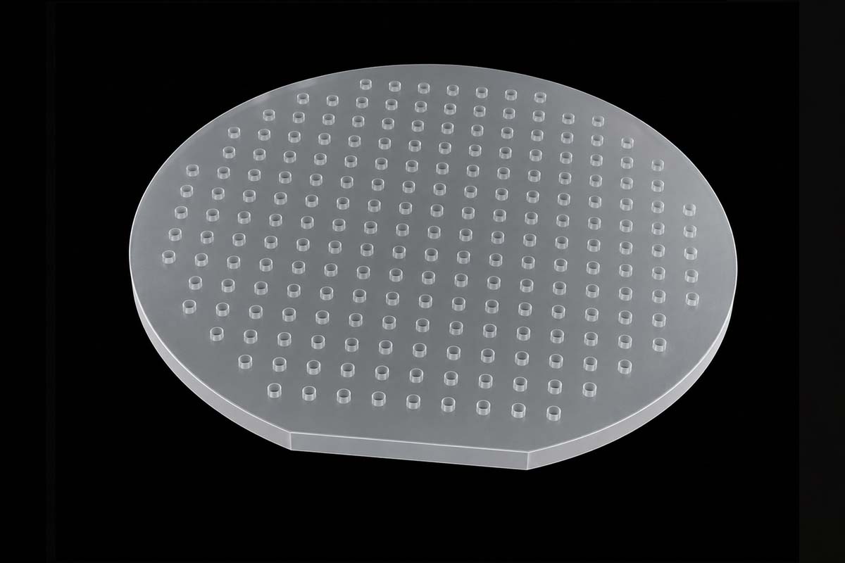
Silicon Through Holes & Bosses
Silicon substrates can be processed with through holes together with raised boss structures for custom MEMS and packaging designs.
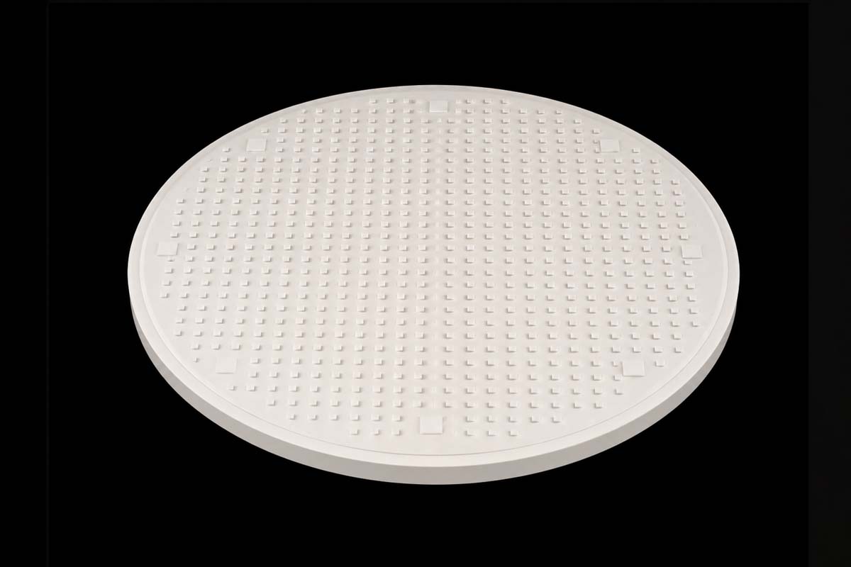
Ceramic Bump Structures
Precision bump and patterned structures can be fabricated on ceramic substrates, including large-format wafer processing.
Need Help?
Send us your substrate material and structure drawing for a process feasibility review.
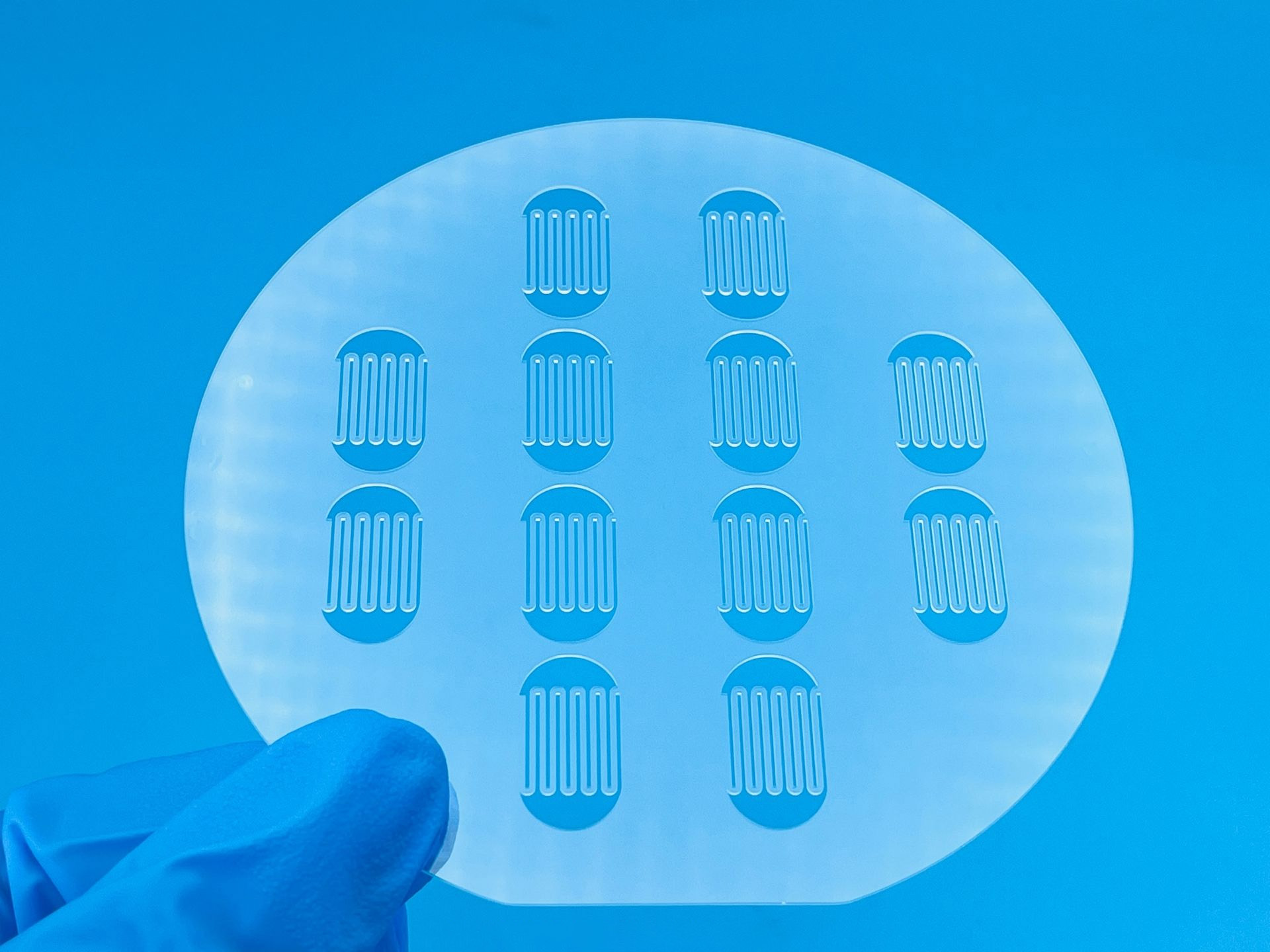
Custom Microstructure Processing
TGVGlass manufactures microstructures according to customer drawings rather than fixed standard geometries.
Our processing platform supports glass, silicon, ceramic and sapphire substrates, allowing different materials and structural features to be combined with the requirements of MEMS, microfluidics, RF devices, optical components and advanced packaging.
Available structures include through holes, blind holes, grooves, microchannels, cavities, oblique holes and custom patterns.
Custom Specification
Material, format, process route and dimensional requirements configured to the customer drawing.
| Parameter | Capability |
|---|---|
| Materials | Glass, silicon, ceramic, sapphire and other technical materials |
| Wafer Size | 2 in., 4 in., 6 in., 8 in., 12 in. |
| Panel Size | ≤510 × 510 mm |
| Substrate Thickness | 100–4800 μm |
| Process Routes | Dry processing, wet processing, sandblasting |
| Structures | Through holes, blind holes, grooves, oblique holes and custom microstructures |
| Line Width / Spacing | >30 μm |
| Tolerance | Within ±5 μm |
| Geometry | Custom according to drawing |
Latest Microstructure Projects
Representative glass, silicon and ceramic structures manufactured for fluidic, optical, MEMS and packaging applications.
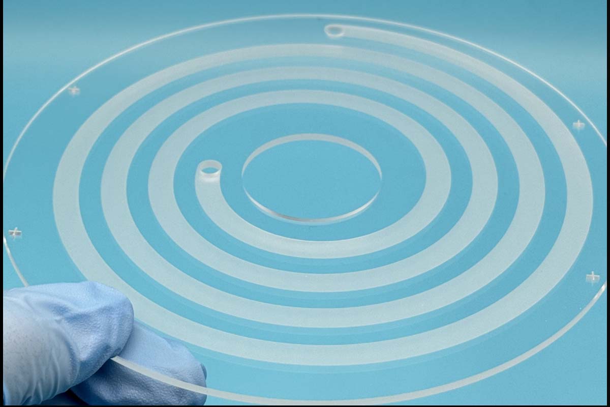
Glass Groove Processing
Precision groove structures fabricated in glass substrates for microfluidic, sensor and packaging applications.
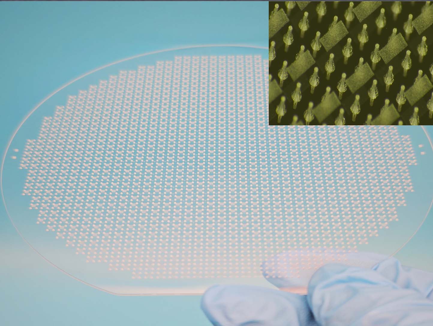
Glass Oblique Hole Processing
Dense arrays of angled holes fabricated according to custom substrate and device requirements.
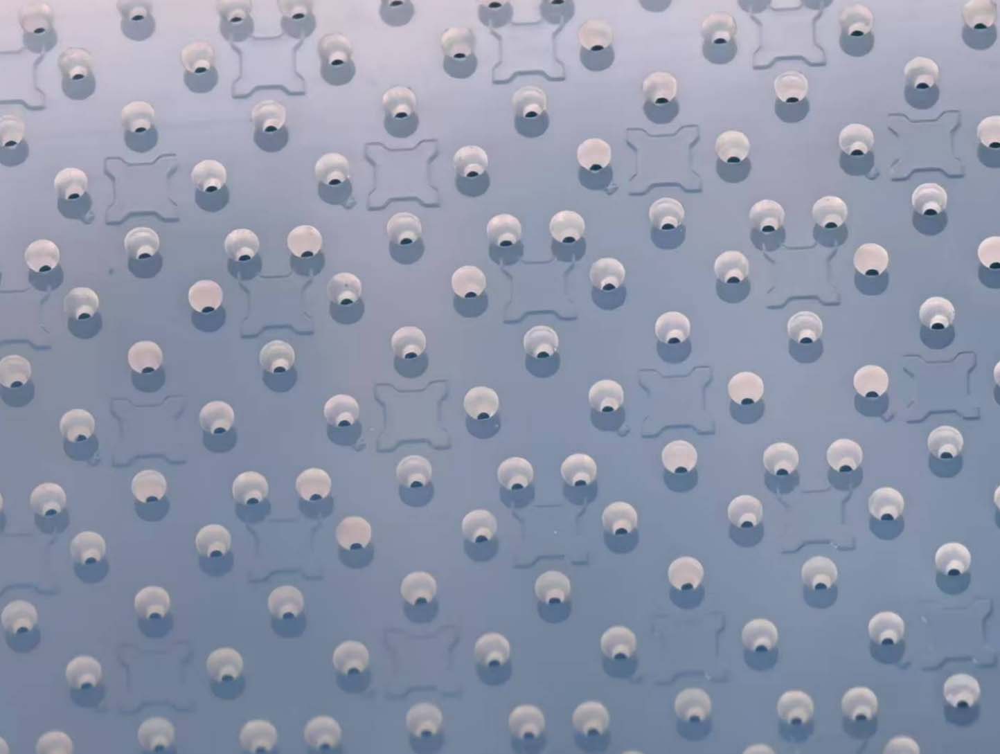
Groove + Through-Hole Structures
Multiple microstructure types can be integrated into the same glass substrate where the design requires both recessed and through features.
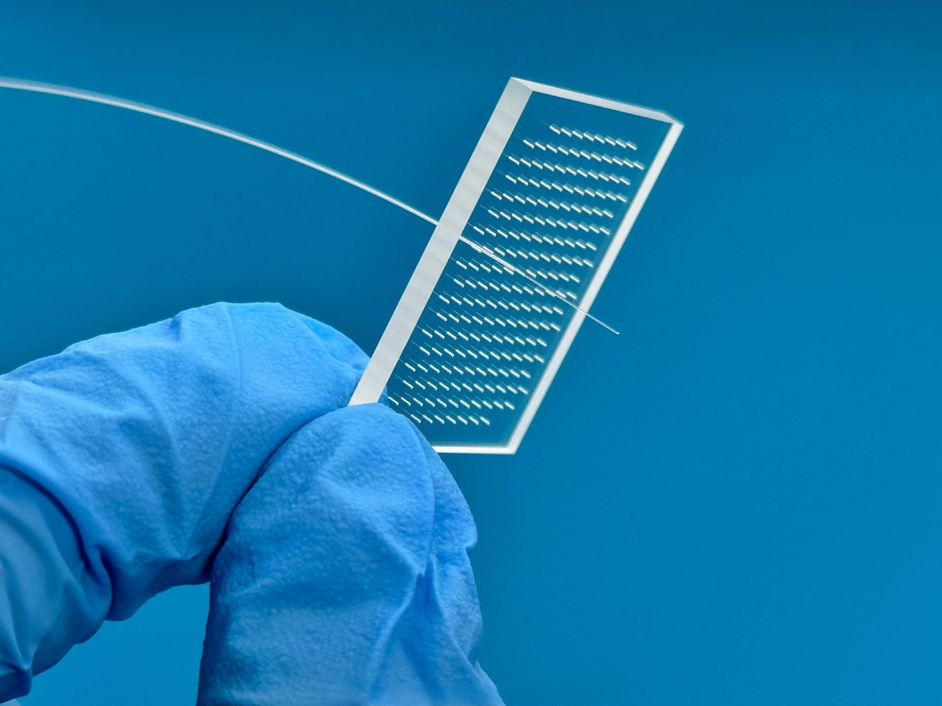
Glass Fiber Insertion Structures
Precision glass microholes can be combined with optical fibers for positioning and optical-device integration.
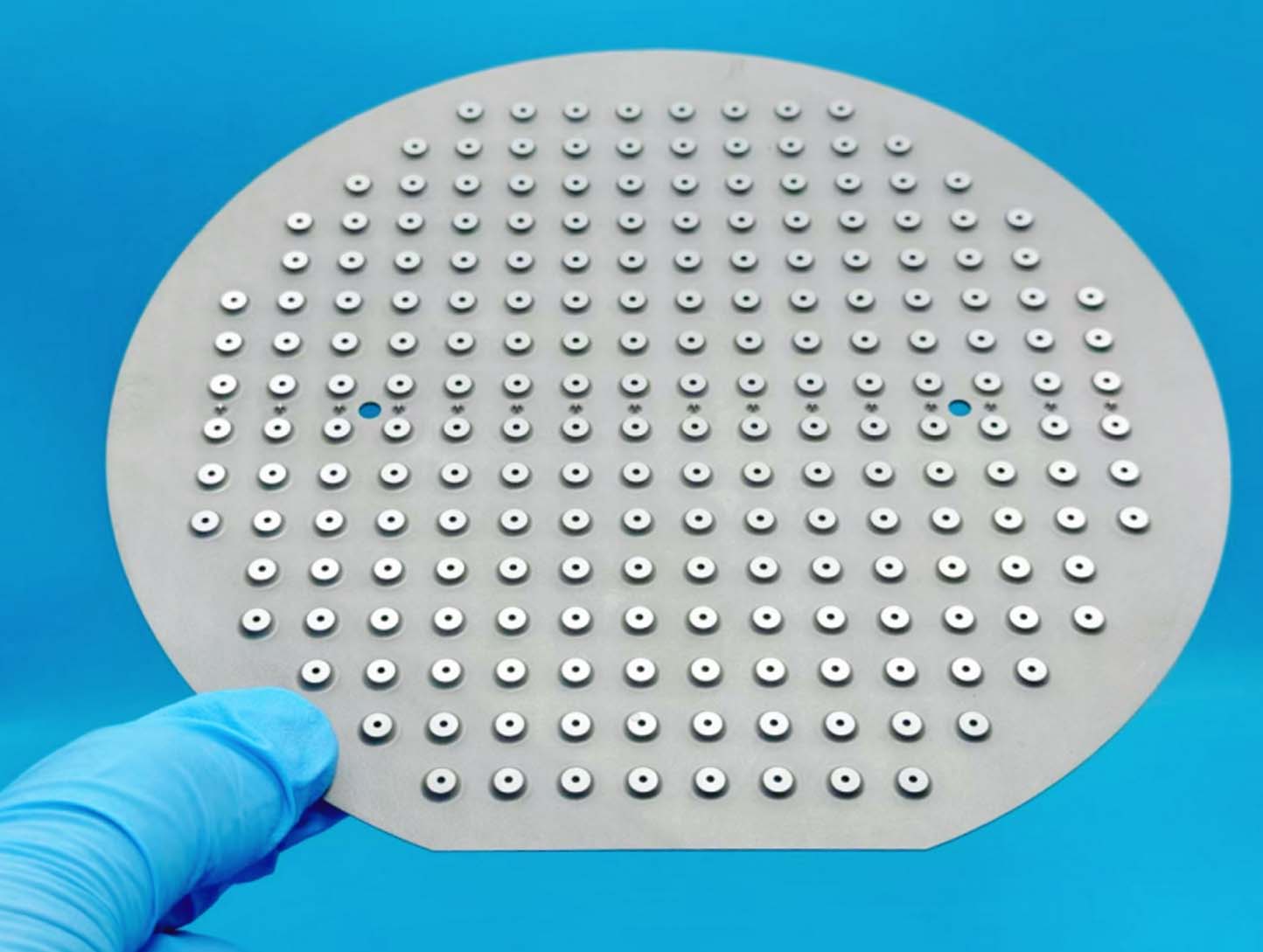
Silicon Through Holes + Bosses
Through-hole and raised silicon structures can be fabricated together for MEMS and semiconductor device designs.
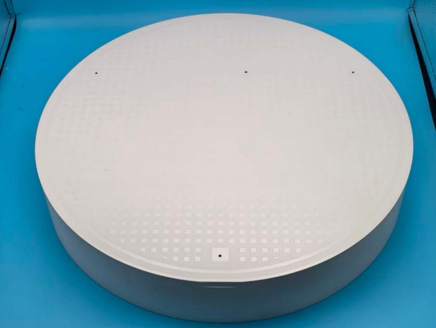
12-Inch Ceramic Bump Processing
Large-format ceramic wafers can be processed with patterned bump structures for custom electronic and packaging applications.
Applications
Precision substrate structures for fluidic, sensor, semiconductor and optical device integration.
Microfluidic Chips
Grooves, microchannels, holes and cavities can be integrated into glass substrates for fluid handling and analysis.
MEMS & Pressure Sensors
Glass and silicon microstructures can be fabricated for sensor cavities, through holes, alignment structures and wafer-level devices.
RF & Semiconductor Devices
Precision substrate structures can support RF chips, semiconductor packaging and other devices requiring custom microfabricated geometries.
Optical & Photonic Devices
Glass holes and alignment structures can be used for optical fibers and other precision photonic assemblies.
Connect with Our Experts
We’re Here to Help
Our engineers review your drawing, material, tolerances, and target quantity before quotation.
Request a Process Evaluation
Send us your substrate material, wafer or panel size, thickness, structure drawing, feature dimensions, tolerance and intended application.