Integrated Glass-Based Packaging
Glass-based packaging combines precision glass microstructures with electrical interconnection, surface routing, bonding and device integration.
TGVGlass supports the key processes required to transform a glass substrate into a functional packaging structure — from microvia formation and conductive via filling to surface circuits, multilayer RDL, wafer bonding, chip dicing and final testing.
Different process combinations are selected according to the substrate structure, interconnection requirements and final device architecture.
Glass-Based Packaging Capabilities
| Process | Capability |
|---|---|
| Glass Microvia | Through vias, blind vias and custom TGV structures |
| Microvia Filling | Paste filling and electroplating-based filling |
| Surface Routing | TGV substrate circuits and glass surface RDL |
| Multilayer Interconnect | Multilayer RDL routing and bump structures |
| Bonding | Laser welding, anodic bonding, Au-Au bonding |
| Dicing | TGV wafer and packaged chip dicing |
| Testing | Electrical, mechanical and hermetic testing |
| Packaging | Custom glass-based wafer-level packaging |
Our Glass-Based Packaging Technologies
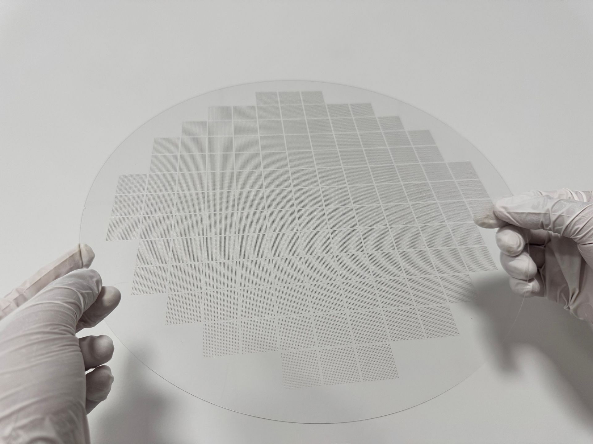
Glass Microvia Formation
Precision microvias are formed in glass substrates to create the vertical structures required for TGV interconnection and advanced packaging.
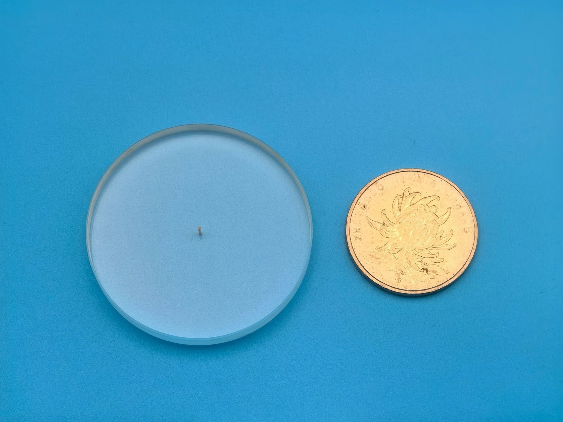
Microvia Metal Filling
Through vias and blind vias can be filled using paste-based or electroplating-based processes to form conductive vertical interconnects.
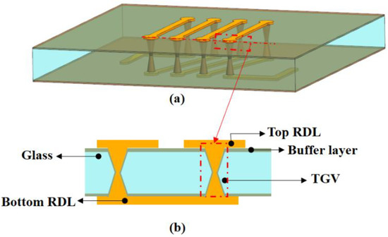
Glass Surface RDL Routing
Redistribution layers and substrate circuits can be fabricated on the glass surface to route electrical connections between TGV vias, device interfaces and package terminals.
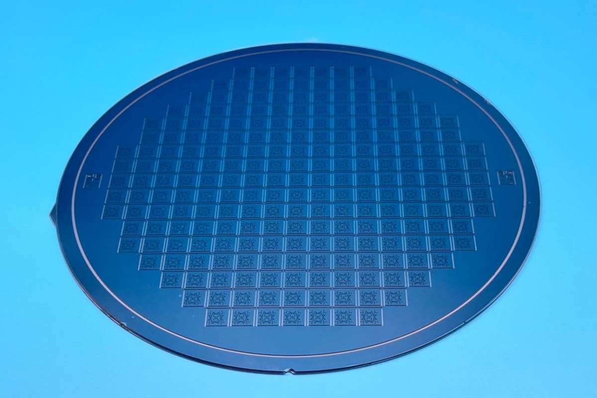
Wafer Bonding
Different bonding technologies are available according to the material combination and package structure, including laser welding, anodic bonding and Au-Au bonding.
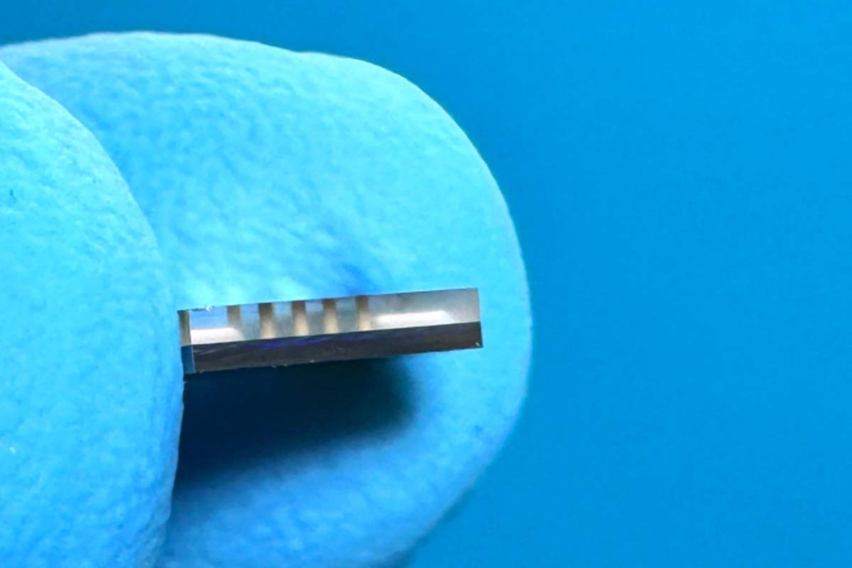
Dicing
TGV wafers and packaged structures can be diced into individual chips or components after wafer-level processing.
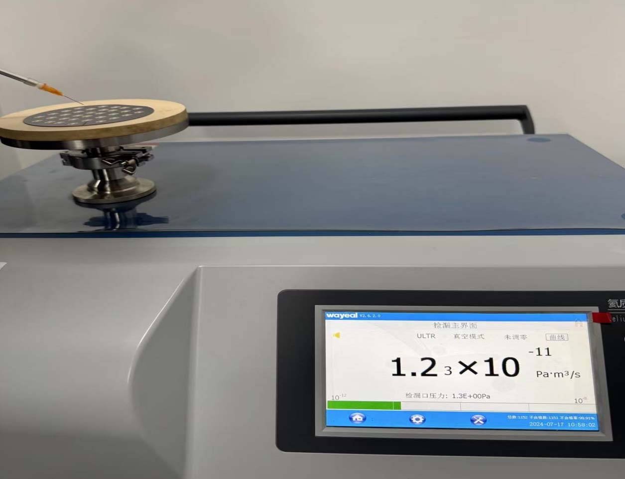
Performance Testing
Electrical, mechanical and hermetic testing can be used to verify the finished packaging structure according to project requirements.
Need Help?
Send us your package architecture and performance requirements to identify the required TGV, RDL, bonding, and test processes.
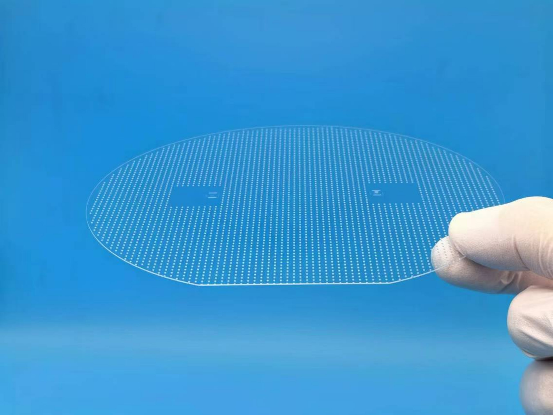
Custom Glass-Based Packaging
TGVGlass develops packaging structures according to the customer’s substrate, device layout and integration requirements.
A project may use only selected process steps or combine multiple technologies into a complete wafer-level packaging route.
Available Process Modules
- Glass microvia formation
- Microvia metal filling
- TGV substrate surface circuits
- Glass surface RDL routing
- Multilayer RDL
- Bump structures
- Laser welding
- Anodic bonding
- Au-Au bonding
- Wafer and chip dicing
- Electrical testing
- Mechanical testing
- Hermetic testing
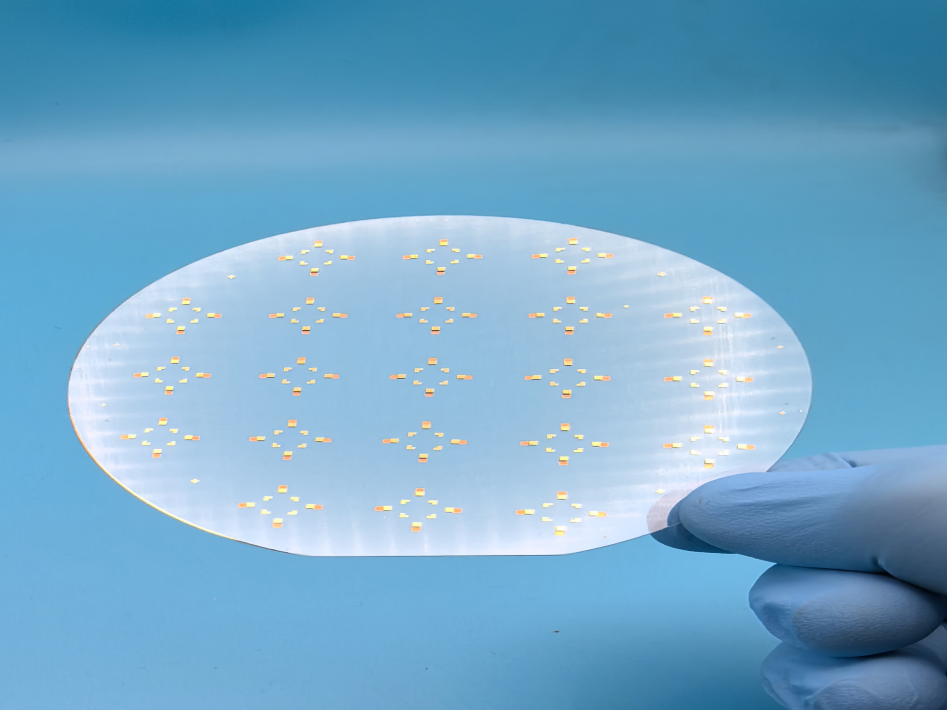
Surface RDL & TGV Substrate Circuits
Surface routing connects the vertical TGV interconnects to device pads, package interfaces and other electrical structures on the glass substrate.
TGVGlass supports TGV substrate surface circuits together with multilayer RDL routing and bump structures as part of the overall glass-based packaging process.
By integrating surface routing with microvia formation and via filling, both vertical and horizontal electrical interconnection can be implemented within the same glass-based package architecture.
Bonding Technologies
Laser Welding
Laser welding is available for selected glass-based packaging and sealing structures.
Anodic Bonding
Anodic bonding can be used for suitable glass and silicon structures in wafer-level packaging.
Au-Au Bonding
Gold-to-gold bonding is available for package structures requiring metallic bonding interfaces.
Testing & Verification
Electrical Testing
Electrical performance can be evaluated after interconnection and packaging.
Mechanical Testing
Mechanical testing is used to evaluate the structural performance of packaged components.
Hermetic Testing
Hermeticity testing is available for package structures requiring controlled sealing performance.
Applications
Integrated glass microvias, routing, bonding and testing for advanced device and wafer-level packaging.
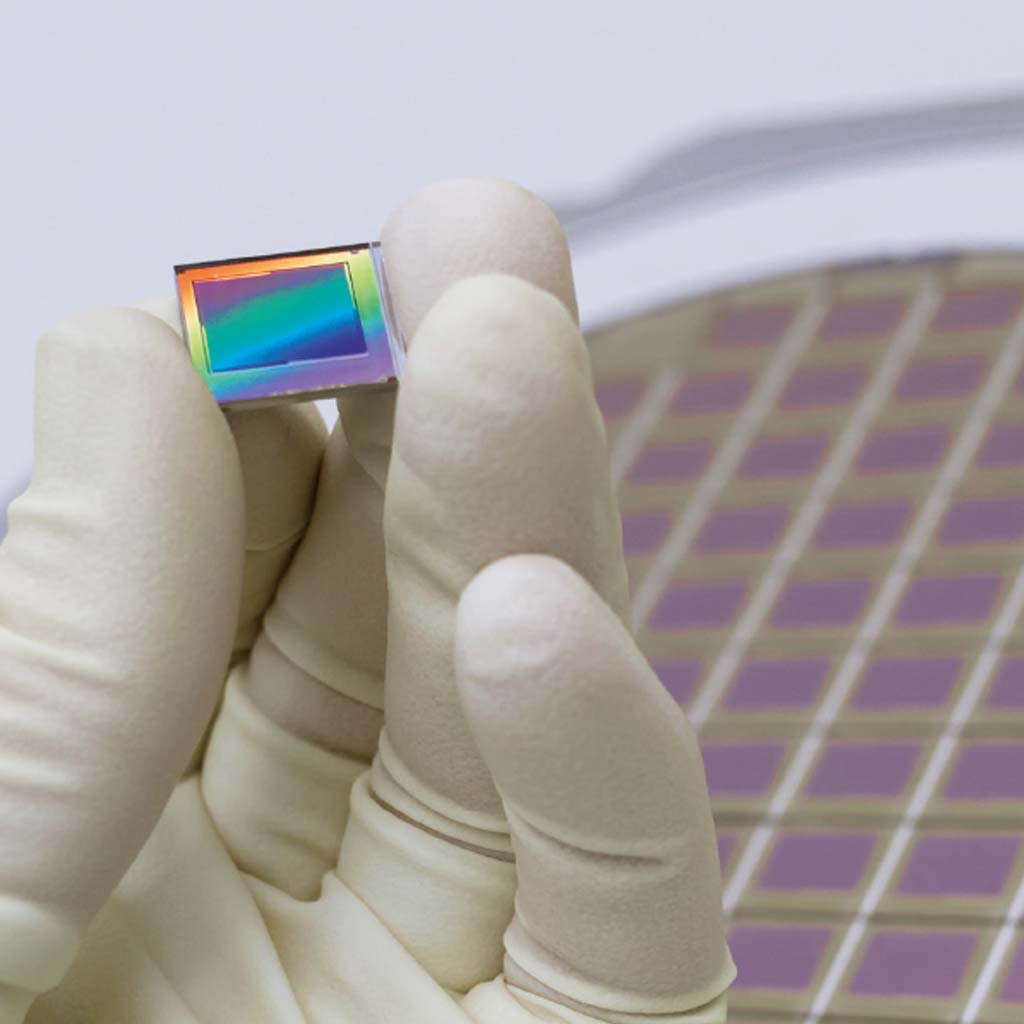
MEMS & Sensors
Glass microvias, surface routing, bonding and hermetic testing are combined for MEMS and sensor wafer-level packaging.
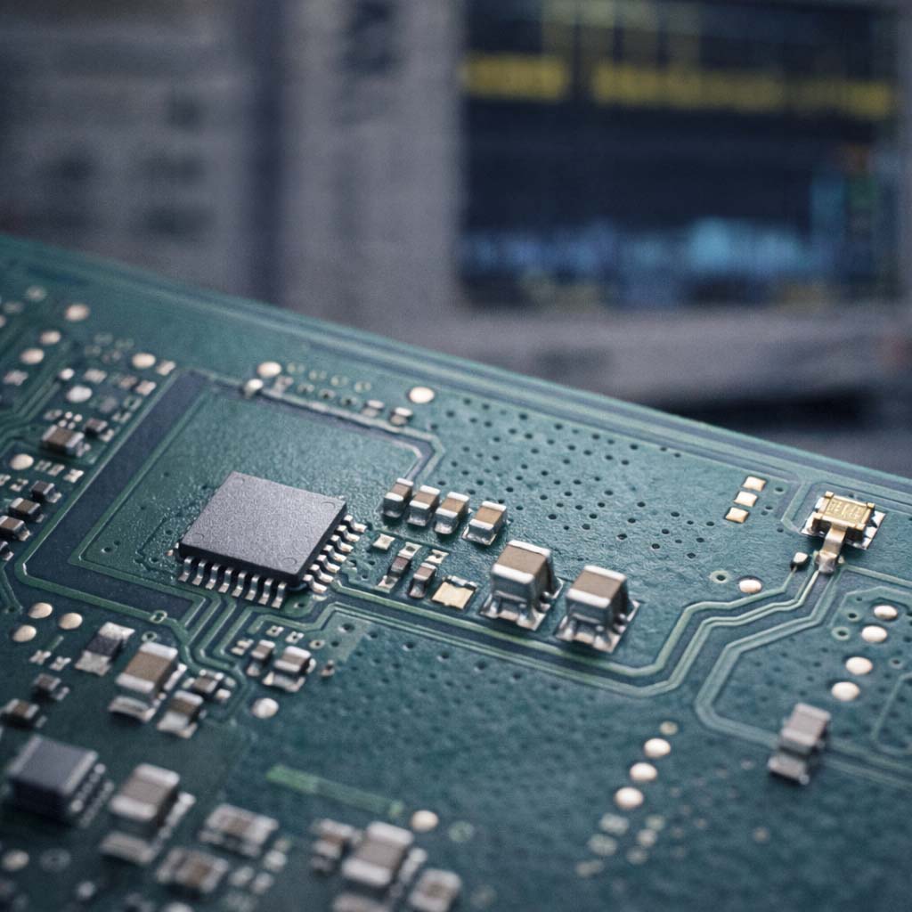
RF & High-Frequency Devices
TGV vertical interconnects and glass surface circuits support compact RF and high-frequency packaging architectures.
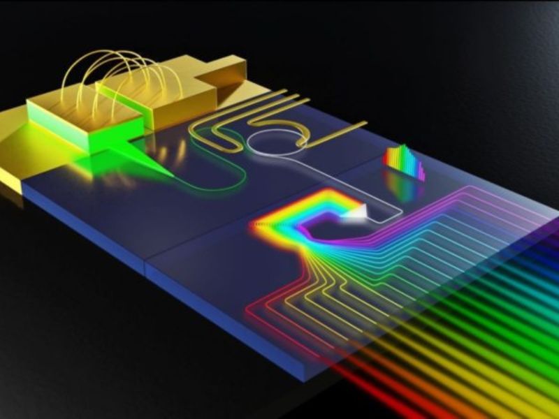
Optical Communication & CPO
Glass-based packaging can integrate precision glass structures with electrical routing for optical communication and CPO devices.
Vacuum Devices
Bonding and hermetic testing can be incorporated into packaging structures intended for vacuum-device applications.
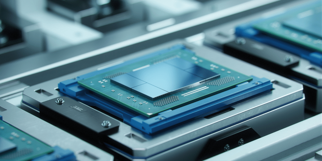
Advanced Semiconductor Packaging
Microvia formation, metal filling, RDL routing and bonding can be combined to create customized three-dimensional glass-based packaging structures.
Connect with Our Experts
We’re Here to Help
Our engineers review your drawing, material, tolerances, and target quantity before quotation.
Request a Process Evaluation
Send us your substrate material, device layout, via structure, interconnection requirements, bonding method, testing requirements and final application.