Through Glass Via (TGV) technology creates vertical electrical interconnects directly through a glass substrate, giving chip packages a lower-loss, more thermally stable alternative to silicon interposers. As 5G, AI accelerators, and high-density MEMS sensors push packaging toward finer pitches and higher frequencies, TGV has moved from a research topic to a mainstream part of the advanced packaging roadmap. This guide walks through how TGV works, how it’s manufactured, and where it’s used.
Key Takeaways
- A TGV is a vertical conductive channel formed through a glass wafer or panel, functionally similar to a through-silicon via (TSV) but built in an insulating rather than semiconducting material.
- Glass offers low dielectric loss, a tunable coefficient of thermal expansion (CTE), excellent dimensional stability, and the ability to be processed in large panel formats — advantages that are hard to match with silicon or organic substrates.
- Via formation methods include laser drilling, laser-induced deep etching (LIDE), photosensitive glass patterning, electrochemical discharge machining, and abrasive jet micromachining, each with different cost, precision, and throughput trade-offs.
- After the via is formed, it must be metallized — typically with an electroless seed layer followed by electrolytic copper plating and chemical mechanical planarization (CMP).
- Typical wafer-level TGVs range from roughly 10-100 µm in diameter with aspect ratios that can reach into the tens; sensor and larger-format packages may use vias above 300 µm with lower aspect ratios.
- TGV is central to RF front-end modules, MEMS/sensor packaging, glass interposers for 2.5D/3D integration, and increasingly photonic packaging.
- Because glass is brittle and has no plastic deformation range, handling, crack control, and yield across large panels remain the main manufacturing challenges.
What Is a Through Glass Via?
Definition and Basic Structure
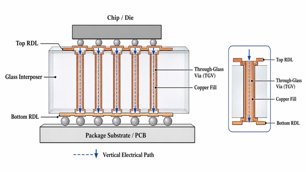
A through glass via is a conductive path — usually copper — that runs from one face of a glass substrate to the other, allowing an electrical signal or power connection to pass vertically through material that would otherwise be a pure insulator. In a finished package, TGVs let designers route signals from a chip on one side of a glass interposer or glass core substrate to a printed circuit board or another die on the other side, without routing everything around the edges of the substrate.
The basic structure has three parts: the glass substrate itself, the via hole formed through it, and the metal fill or metal lining that makes the via electrically conductive. Depending on the application, a via can be fully filled with copper (a “filled” via, preferred for structural strength and thermal performance) or only lined along its walls (a “conformal” via, which uses less metal and can reduce stress).
How TGV Compares to TSV
TGV is often introduced alongside through-silicon via (TSV) technology because the two solve the same basic problem — vertical interconnection through a substrate — using different base materials. Silicon is a semiconductor, so a TSV needs an insulating liner between the copper and the silicon to prevent signal leakage and parasitic capacitance. Glass is a natural insulator, so a TGV doesn’t need that extra liner step, which can simplify the process stack. Glass also tends to have lower electrical loss at high frequencies than silicon, which is one reason TGV has gained traction in RF and mmWave applications. The trade-off is that glass’s brittleness introduces its own handling and process-control challenges that silicon, as a more mechanically forgiving material, doesn’t have to the same degree. A closer side-by-side comparison of cost, performance, and process maturity deserves its own article — this guide focuses on TGV specifically.
Why Glass? Material Advantages for TGV
Electrical and RF Performance
Glass is an excellent electrical insulator with low dielectric loss, which translates directly into lower signal attenuation for the high-frequency circuits used in 5G and other RF applications. Because the substrate itself doesn’t need an isolation layer the way silicon does, the parasitic capacitance around each via can be lower, which helps preserve signal integrity as pitches shrink.
Thermal and Mechanical Properties
Unlike silicon, glass compositions can be tuned to match the coefficient of thermal expansion (CTE) of the components mounted on them, which reduces the mechanical stress that builds up during temperature cycling and improves long-term reliability. Glass also offers strong chemical resistance and can be hermetically sealed, which matters for MEMS sensors and RF filters that need a protected cavity.
Panel-Scale Manufacturing
Glass suppliers such as Corning, Asahi, and Schott can produce panels well over a meter on a side, and thin glass sheets below 50 µm are commercially available alongside thicker material up to several millimeters. That panel-scale availability is what allows TGV processing to move beyond round wafers into large rectangular panels, which is one of the arguments for glass’s long-term cost advantage over silicon interposers — provided defect rates can be kept under control as panel size grows.
How TGV Is Made: The Manufacturing Process
Via Formation Methods
Because glass has essentially no plastic deformation range — it cracks rather than bends under stress — forming a via is more delicate than drilling through organic laminate or copper. Several methods have been developed, each suited to different via sizes and glass types:
- Laser drilling / laser ablation — a focused laser removes material directly to form the hole. It’s fast and flexible but can leave debris and micro-cracking that needs to be managed.
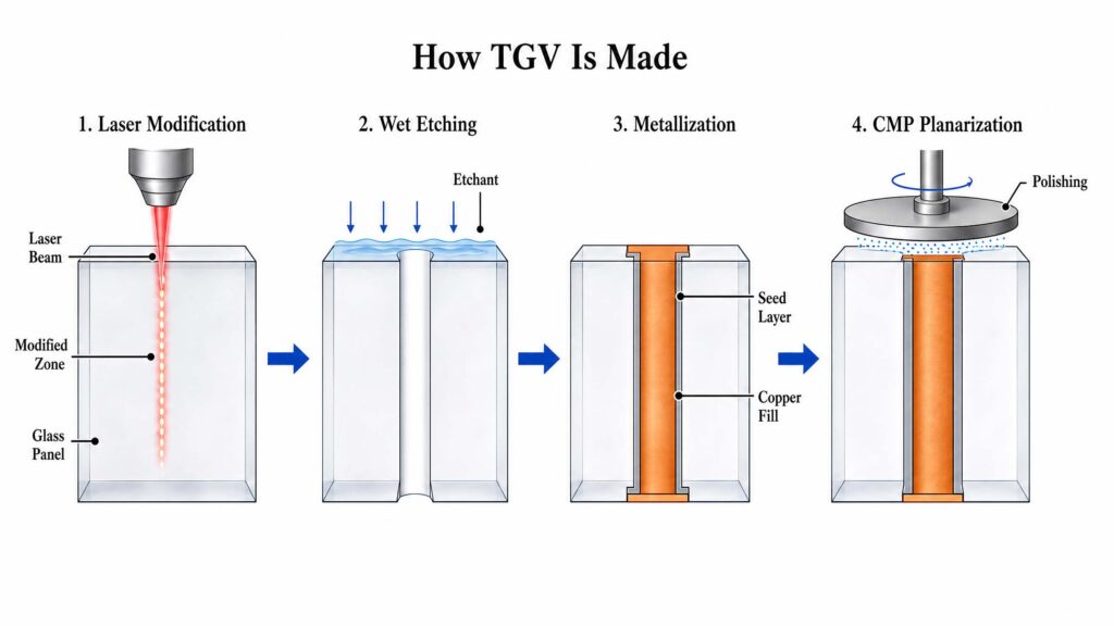
- Laser-induced deep etching (LIDE) — a two-step process. An ultrashort-pulse laser first modifies the glass along a defined path (a highly localized change, often only a few microns wide, that runs the full thickness of the panel without removing material or cracking it), then the panel is immersed in a chemical etchant such as hydrofluoric acid or a hot alkaline solution, which etches away the modified glass much faster than the surrounding bulk material to open the via.
- Photosensitive glass patterning — a photomask and UV exposure create a latent image in specially formulated glass, which is then heat-treated to crystallize the exposed areas before wet etching removes them. This method can pattern many vias simultaneously without a laser.
- Electrochemical discharge machining and abrasive jet micromachining — mechanical or discharge-based material removal methods that are typically used for larger via sizes or specific glass types where laser and photosensitive methods are less practical.
The resulting via shape is often hourglass-shaped when etched or drilled from both sides, though some manufacturers are working toward more cylindrical profiles for better metal fill and more predictable electrical performance.
Via Metallization
Once the hole exists, it has to be turned into a conductor. The typical sequence is:
- Seed layer deposition — an electroless metal layer (commonly nickel or copper) is deposited to coat the via walls and make them conductive enough for the next step.
- Electrolytic copper plating — copper is electroplated onto the seed layer to either line the via walls or fully fill the via, depending on the design.
- Chemical mechanical planarization (CMP) — the top and bottom surfaces of the panel are polished flat to remove excess copper and create a smooth surface for the redistribution layer (RDL) that follows.
TGV-First vs. TGV-Last Integration
Manufacturers generally choose between forming the vias before building up the circuit layers on the glass (“TGV-first”) or after (“TGV-last”). TGV-first keeps the metallized via as a stable base for subsequent processing, while TGV-last can simplify handling of very thin or large-format panels by delaying the more delicate via-fill step. The choice affects cost, cycle time, and which defects are easiest to catch and rework.
Key Design Parameters
Via Diameter, Pitch, and Aspect Ratio
Via diameter and aspect ratio (via depth divided by via diameter) are the two parameters that most directly set the difficulty and cost of a TGV process. Wafer-level TGVs for advanced packaging commonly fall in the roughly 10-100 µm diameter range, with aspect ratios that can extend well beyond 10:1 depending on the formation method. Larger-format sensor or MEMS packages, where routing density matters less than mechanical robustness, may use vias above 300 µm with aspect ratios below 1. Tighter pitch — the center-to-center spacing between adjacent vias — increases routing density but also increases the risk of crack propagation between neighboring vias, so pitch and aspect ratio are usually optimized together rather than independently.
Via Shape and Taper Control
An hourglass or tapered via profile is easier to achieve with etch-based processes but can complicate uniform metal fill, since the narrowest point of the via is the hardest section to plate completely. Controlling taper angle — and, where possible, moving toward straighter via walls — is an active area of process development because it directly affects fill quality, electrical resistance consistency, and long-term reliability under thermal cycling.
Applications of TGV Technology
RF and 5G Front-End Modules
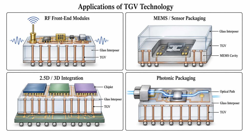
Glass’s low dielectric loss makes TGV-based substrates attractive for RF filters, front-end modules, and other components that need to preserve signal integrity at millimeter-wave frequencies. TGV also supports hermetic wafer-level packaging for devices like RF filters, where the package needs to protect a sensitive resonator cavity while still bringing signals out through the substrate.
MEMS and Sensor Packaging
MEMS sensors — accelerometers, gyroscopes, pressure sensors, and similar devices — often need a hermetically sealed cap bonded over the moving structure. Glass is a natural fit because it can be anodically bonded to silicon and can carry TGVs to route the sensor’s electrical signals out through the cap without breaking the seal.
Glass Interposers for 2.5D/3D Integration
As an alternative to silicon interposers in 2.5D and 3D chip stacking, glass interposers use TGVs to connect multiple dies mounted side by side or stacked vertically. The combination of a tunable CTE, low electrical loss, and large panel availability is part of why glass interposers are increasingly discussed as a path to lower-cost advanced packaging at scale.
Photonic and Optical Packaging
Glass is already the substrate of choice for many optical components, so extending it with TGVs allows electrical and optical functions to be combined on the same platform — useful for photonic interposers and optical transceiver packaging where both light and electrical signals need to be routed through the same substrate.
Manufacturing Challenges
TGV’s biggest advantages — an insulating, thermally stable, large-format substrate — come with a corresponding set of manufacturing challenges. Glass’s brittleness means that voids, micro-cracks, and uncontrolled taper are ever-present risks at every step, from laser modification through etching, plating, and planarization. As panel sizes grow to capture glass’s cost advantages, the probability of at least one yield-limiting defect on a given panel also grows, so defect density has to improve at least as fast as panel area does for panel-level TGV processing to deliver on its cost promise. Handling thin, large glass panels without cracking them — and keeping copper fill void-free inside high-aspect-ratio vias — remain the process areas that most determine how quickly TGV moves from advanced R&D lines into high-volume production.
Through Glass Via technology addresses a real bottleneck in advanced packaging: how to route dense, high-frequency signals through a substrate without paying the electrical and thermal penalties that come with silicon. Its combination of low dielectric loss, tunable CTE, and large-panel scalability explains why it’s found a home in RF modules, MEMS packaging, and next-generation interposers. The remaining work is mostly about manufacturing discipline — getting via formation, metallization, and panel handling to scale in yield the same way they’ve already scaled in capability.
FAQ
What does TGV stand for? TGV stands for Through Glass Via — a vertical electrical connection formed through a glass substrate.
Is TGV the same as TSV? No. Both provide vertical interconnects through a substrate, but TSV (through-silicon via) uses silicon and requires an insulating liner, while TGV uses glass, which is already an insulator. The materials, process steps, and typical applications differ even though the end goal — vertical interconnection — is the same.
What is the smallest via size possible with TGV? It depends on the formation method and glass type, but wafer-level processes commonly achieve via diameters in the tens of microns, with laser-based and photosensitive glass methods generally capable of finer features than mechanical or discharge-based methods.
Why is glass considered better than silicon for RF applications? Glass has lower dielectric loss than silicon, which means signals passing through or near the substrate lose less energy — an important advantage at the high frequencies used in 5G and mmWave systems.
What is laser-induced deep etching (LIDE)? LIDE is a two-step via formation process in which an ultrashort-pulse laser first modifies the glass along the via path without removing material, and the panel is then chemically etched so the modified glass dissolves much faster than the surrounding material, opening a clean via through the full thickness of the panel.
Can TGV vias be fully filled with copper? Yes. Vias can be either fully filled with electroplated copper for maximum conductivity and structural strength, or lined along the walls only, depending on the design’s electrical and mechanical requirements.
What industries use TGV technology today? TGV is used in RF front-end modules and 5G components, MEMS and sensor packaging, glass interposers for 2.5D/3D semiconductor integration, and increasingly in photonic and optical packaging.
What is the biggest manufacturing challenge for TGV? Glass’s brittleness. Because it has no plastic deformation range, every process step — laser modification, etching, plating, and planarization — carries a risk of cracking or void formation, and controlling that risk while scaling to larger panel sizes is the main challenge to high-volume production.