Both through-silicon vias (TSV) and through-glass vias (TGV) solve the same basic problem — routing signals vertically through a substrate instead of around its edges — but they start from opposite materials and inherit very different strengths and limits as a result. TSV uses silicon, the material the rest of the chip is already made from; TGV uses glass, a natural insulator with very different mechanical behavior. This guide compares how each is made, what they cost to manufacture, and where their performance diverges, so you can see which one fits a given packaging problem.
| Feature | TSV (Through-Silicon Via) | TGV (Through-Glass Via) |
|---|---|---|
| Base material | Silicon (semiconductor) | Glass (insulator) |
| Needs an insulating liner | Yes — silicon conducts, so vias need isolation | No — glass is already an insulator |
| Typical via formation | Deep reactive-ion etching (DRIE) | Laser drilling, LIDE, or photosensitive glass patterning |
| Substrate format | Round wafers (200/300 mm) | Round wafers or large rectangular panels |
| High-frequency signal loss | Higher, due to silicon’s semiconducting bulk | Lower, due to glass’s low dielectric loss |
| CTE matching | Fixed by silicon’s properties | Tunable via glass composition |
| Process maturity | Mature, in high-volume production for over a decade | Newer, moving from R&D into volume production |
| Typical strongest use case | High-density logic and memory stacking (e.g., HBM) | RF/mmWave modules, sensors, optical and glass interposers |
Key Takeaways
- TSV and TGV both create vertical electrical paths through a substrate, but TSV uses silicon and TGV uses glass — a difference that shapes nearly everything else about the two technologies.
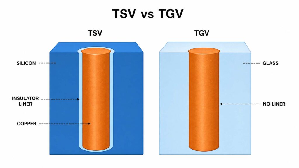
- Because silicon is a semiconductor, TSV requires an extra insulating liner inside each via to prevent current leakage and crosstalk; glass doesn’t need this step since it’s already an insulator.
- TSV is typically formed by deep reactive-ion etching; TGV is typically formed by laser drilling, laser-induced deep etching (LIDE), or photosensitive glass patterning.
- Glass’s ability to be processed in large rectangular panels — not just round wafers — is one of the main structural reasons TGV is discussed as a lower-cost path at scale.
- TSV remains the mature, high-density choice for logic and memory stacking, such as high-bandwidth memory (HBM).
- TGV’s lower dielectric loss gives it an edge in RF, mmWave, and other high-frequency applications where silicon’s signal loss and crosstalk become limiting factors.
- Glass’s tunable coefficient of thermal expansion (CTE) helps reduce warpage in large panels, while silicon’s CTE is fixed by the material itself.
- Neither technology is a universal replacement for the other — the right choice depends on whether the priority is interconnect density and process maturity (TSV) or high-frequency performance and large-format cost efficiency (TGV).
What Is TSV?
Definition and Structure
A through-silicon via is a vertical conductive path etched through a silicon wafer, most often filled or lined with copper, that connects circuitry on one side of the wafer to the other or links stacked dies together. Because silicon is a semiconductor rather than an insulator, every TSV needs a thin dielectric liner between the copper and the surrounding silicon; without it, current would leak into the substrate and interfere with neighboring circuits.
Manufacturing Process
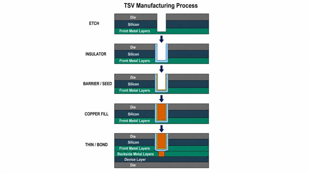
TSV fabrication generally follows a sequence of deep etch, liner deposition, and metal fill:
- Via etching — deep reactive-ion etching (DRIE), commonly using the Bosch process, cuts a high-aspect-ratio hole into the silicon wafer.
- Insulating liner deposition — a dielectric layer (typically an oxide) is deposited to coat the via walls and electrically isolate the eventual copper fill from the silicon.
- Barrier and seed layer — a diffusion barrier and a conductive seed layer are added on top of the liner to prepare the via for plating.
- Copper fill — the via is filled by electroplating, and excess copper is removed by chemical mechanical planarization (CMP).
- Wafer thinning and bonding — the wafer is thinned to expose the bottom of the vias, then bonded to other dies or wafers to complete the stack.
TSV processes are generally split into “via-first,” “via-middle,” and “via-last” approaches, depending on whether the vias are formed before, during, or after the front-end transistor processing — a choice that affects which fab handles which step and how the process integrates with existing CMOS lines.
Common Uses
TSV is the interconnect behind high-bandwidth memory (HBM), where multiple DRAM dies are stacked and connected through vias to deliver more bandwidth per watt than side-by-side memory chips. It’s also used in CMOS image sensors, where TSVs route signals from the front-side sensor to backside pads without the wire bonds that would otherwise complicate a compact camera module, and in 2.5D interposers that sit between multiple logic and memory dies on a package substrate.
What Is TGV?
Definition and Structure
A through-glass via is the same basic idea — a vertical conductive path through a substrate — built in glass instead of silicon. Because glass is already an electrical insulator, the copper (or other metal) fill can sit directly against the glass walls without a separate isolation layer, which removes a full process step compared to TSV.
Manufacturing Process
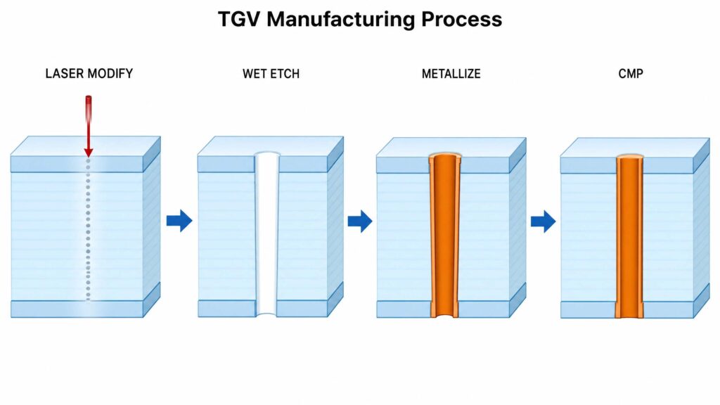
TGV fabrication centers on forming a clean via in a brittle material and then metallizing it:
- Via formation — commonly done by laser drilling, laser-induced deep etching (LIDE), or photosensitive glass patterning, with via diameters typically in the range of roughly 20-150 µm depending on the method and glass type.
- Seed layer deposition — a thin conductive layer, often applied by sputtering or an electroless process, coats the via walls.
- Metal electroplating — copper (or a nickel-copper combination) is electroplated to fill or line the via.
- Planarization — the panel surfaces are polished flat by CMP to prepare for the redistribution layer that follows.
Because glass doesn’t need the liner-deposition step that silicon requires, and because TGV panels can be processed at much larger sizes than round silicon wafers, the overall process has fewer steps and can cover more usable area per production run.
Common Uses
TGV shows up most often where high-frequency performance or hermetic sealing matters: RF filters and duplexers, integrated passive devices (IPDs) such as inductors and capacitors built directly into the glass, MEMS and sensor caps that need a sealed cavity, and — increasingly — glass interposers and glass core substrates being evaluated as an alternative to silicon interposers in 2.5D and 3D packaging for high-performance computing and AI accelerators.
Key Differences
Process Differences
The single biggest process difference comes down to that insulating liner. Because silicon conducts, every TSV needs a dedicated dielectric deposition step before metallization can happen; glass skips it entirely, since the bulk material is already insulating. On the other hand, silicon’s mechanical behavior — it can be etched with well-understood, decades-old DRIE recipes — is far more forgiving than glass, which has no plastic deformation range and fractures rather than bends under stress. That trade-off shows up directly in yield management: TSV process control is mostly about etch uniformity and liner quality, while TGV process control is mostly about avoiding cracks, voids, and uncontrolled taper in a brittle material.
Substrate format is the other major process difference. TSV is built on round silicon wafers, typically 200 mm or 300 mm in diameter, matching the rest of standard semiconductor fab equipment. TGV can be processed on round wafers too, but glass’s availability in large rectangular panels — sometimes called panel-level packaging (PLP) — opens a path to covering more usable area per process cycle than a round wafer allows.
Cost Differences
Skipping the insulating-liner step and being able to use large rectangular glass panels instead of round wafers are the two structural reasons TGV is generally discussed as the lower-cost option at scale. Some industry sources describe glass-interposer manufacturing costs as a fraction of comparable silicon-interposer costs, largely attributable to these two factors — though the actual gap in any given program depends heavily on via density, panel yield, and how mature the specific TGV process is at a given supplier. TSV, by contrast, benefits from over a decade of high-volume production experience, which keeps its cost predictable even though the base process has more steps.
Performance Differences
Electrically, the key difference is dielectric loss. Silicon is a semiconductor, and free carriers in the bulk material can interact with the electric fields around a TSV, contributing to signal loss and crosstalk between neighboring vias at high frequencies. Glass has a lower dielectric constant and higher resistivity than silicon, so signals passing near a TGV lose less energy — a meaningful advantage in RF and mmWave applications like 5G front-end modules, where insertion loss and out-of-band rejection are tightly specified.
Thermally and mechanically, TSV inherits silicon’s fixed coefficient of thermal expansion, which can contribute to warpage when a silicon interposer is combined with dies or substrates that expand at different rates during thermal cycling. TGV’s glass composition can be tuned to better match the CTE of surrounding components, which helps control warpage — particularly important as panel sizes grow. Silicon does have the edge in raw interconnect density and via pitch today: TSV processes with via pitches down to the tens of microns (and in some advanced stacks, single-digit microns) are already in production, a density level TGV is still working toward at comparable scale.
Applications: Where Each Technology Excels
TSV remains the default choice wherever interconnect density and process maturity matter most — high-bandwidth memory stacks, CMOS image sensors, and 2.5D logic-plus-memory interposers where the process needs to be proven and repeatable at very high volumes.
TGV is gaining ground fastest in applications where glass’s material properties translate into a direct performance or cost advantage: RF and mmWave front-end modules, integrated passive devices, hermetically sealed MEMS and sensor packages, and — as glass core substrates mature — large-panel interposers for high-performance computing and AI accelerator packages, where panel-level processing offers a path to lower cost per package than round silicon wafers.
How to Choose Between TGV and TSV
The decision usually comes down to which constraint matters more for the specific product: if the application needs the highest possible interconnect density with a manufacturing process that has been proven at high volume for years, TSV is still the safer default. If the application is sensitive to high-frequency signal loss, needs a hermetic seal, or is trying to scale to larger substrate formats at lower cost, TGV’s material properties make it worth serious evaluation — keeping in mind that its supply chain and process maturity are still catching up to TSV’s.
Both technologies continue to develop in parallel rather than one simply replacing the other. TSV’s decade-plus head start in high-density logic and memory stacking isn’t going away, while TGV’s advantages in RF performance, hermetic sealing, and large-panel cost structure are opening use cases that silicon interposers were never well suited for in the first place. Understanding which constraint — density and maturity, or frequency performance and format flexibility — matters most for a given design is the real starting point for choosing between them.
FAQ
What is the main difference between TGV and TSV? TSV uses silicon, which is a semiconductor and needs an insulating liner inside each via. TGV uses glass, which is already an insulator, so it doesn’t need that liner step. This single difference drives most of the other process, cost, and performance differences between the two technologies.
Is TGV cheaper than TSV? TGV is often described as lower-cost at scale because it skips the liner-deposition step and can be processed on large rectangular panels instead of round wafers. The actual cost gap depends on via density, yield, and how mature a given supplier’s TGV process is, so it isn’t a fixed number across all applications.
Which technology has higher interconnect density? TSV currently offers finer via pitch and higher interconnect density in production, since it has been in high-volume manufacturing for over a decade. TGV is improving but hasn’t yet matched TSV’s density at comparable scale.
Why is TGV better for RF and 5G applications? Glass has lower dielectric loss and higher electrical resistivity than silicon, so high-frequency signals passing near a TGV lose less energy and experience less crosstalk than they would near a TSV surrounded by semiconducting silicon.
Can TGV and TSV be used together in the same package? Yes. Some advanced packages combine a TSV-based silicon die or interposer with a TGV-based glass interposer or substrate, using each material where its strengths matter most within the same system.
Which is more mature, TGV or TSV? TSV is significantly more mature, with well-established process flows in high-volume production for memory stacking, image sensors, and logic interposers. TGV is newer and moving from advanced R&D and early production into broader commercial use.
Does TGV or TSV have better thermal reliability? TGV has an advantage in CTE matching, since glass composition can be tuned to reduce the thermal expansion mismatch with surrounding components, which helps control warpage. TSV inherits silicon’s fixed CTE, which is well understood but not adjustable in the same way.
Is TGV expected to replace TSV? Not entirely. TSV is likely to remain the standard for the highest-density logic and memory stacking for the foreseeable future, while TGV is expanding into applications — RF, hermetic sensor packaging, large-panel interposers — where glass’s material properties offer a clearer advantage than silicon’s.