Every through-glass via combines two materials that expand at very different rates when heated: glass, which barely moves, and copper, which expands roughly five to ten times more per degree. That mismatch doesn’t go away just because the bulk glass composition is well chosen — it shows up locally, at the via itself, every time the substrate goes through a thermal cycle, an anneal, or a solder reflow. This guide focuses specifically on how that mismatch translates into real failure modes, what process and design choices make it better or worse, and how it’s tested and modeled before a TGV design goes into production.
Key Takeaways
- Copper’s coefficient of thermal expansion is far higher than glass’s, so even a well-matched bulk substrate still has significant local CTE mismatch at every individual via.
- The main failure modes linked to this mismatch are radial and circumferential glass cracking, copper protrusion out of the via, delamination at the glass-copper interface, and panel-level warpage from mismatch with build-up and redistribution layers.
- Copper protrusion tends to increase with annealing time, though the rate of growth slows the longer annealing continues.
- Heating rate matters in more than one direction: some studies show faster heating increases the probability of radial cracking, while others show slower heating reduces in-plane glass deformation near the via — both point to the same underlying idea that stress has less time to relax when temperature changes quickly.
- Reducing copper fill volume, optimizing via taper, and adding stress-buffering layers are among the main design strategies for managing CTE-related stress.
- Warpage and via-level cracking are related but separate reliability concerns — one is a panel-scale phenomenon driven by mismatch between the glass core and its build-up layers, the other is local to each individual via.
- Finite element analysis is the standard tool for predicting stress distribution and warpage before a design is built, and is typically paired with physical thermal cycling tests to confirm the model.
- CTE mismatch isn’t something a single material choice eliminates — it’s a design and process variable that has to be actively managed through via geometry, fill strategy, and thermal processing conditions.
Why CTE Mismatch Matters in a TGV
The Core Problem: Glass, Copper, and Differential Expansion
A through-glass via is, mechanically, two very different materials bonded together in close contact: a rigid, low-expansion glass wall and a copper fill or lining with a CTE several times higher. Copper’s CTE sits in the range of roughly 17 ppm/°C, while glass substrates used for TGV typically run anywhere from well under 1 ppm/°C (fused silica) to around 3-10 ppm/°C (various borosilicate compositions) — in every case, a large gap. When the substrate heats up, the copper wants to expand far more than the surrounding glass allows, and that resistance generates mechanical stress concentrated right at the via.
This is true no matter how well the bulk glass composition is matched to silicon or to the rest of the package — matching the glass’s overall CTE to a die or a build-up layer says nothing about the CTE mismatch between the glass and the copper sitting directly inside its own vias. That’s why TGV reliability engineering treats via-level thermal stress as its own problem, separate from substrate-level CTE selection.
Where Stress Concentrates
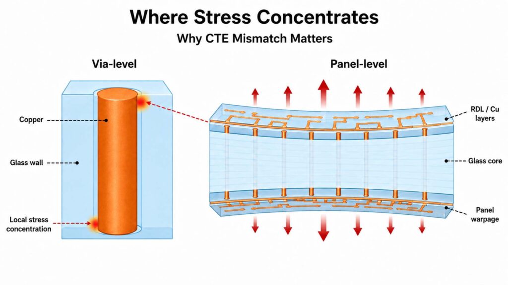
There are really two related but distinct thermal-stress problems in a TGV substrate. The first is local: stress concentrated right at the glass-copper interface inside and immediately around each via, driven by the copper-to-glass CTE mismatch described above. The second is at the panel or substrate scale: warpage driven by the CTE mismatch between the glass core and the dielectric build-up and redistribution layers laminated onto its surface. Both are real reliability risks, but they respond to different design levers — via-level stress is mostly addressed through via geometry and fill strategy, while panel-level warpage is addressed through build-up material selection, layer symmetry, and RDL layer count.
Failure Modes Caused by CTE Mismatch
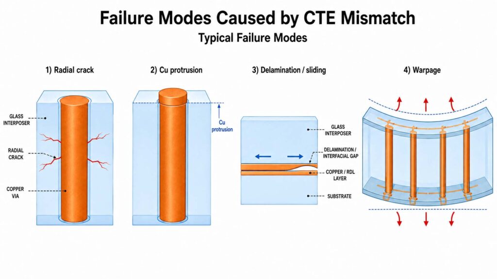
Radial and Circumferential Glass Cracking
When a metallized TGV is heated — during processing steps like post-plating annealing, or later during solder reflow and thermal cycling in the field — the copper’s greater expansion pushes outward against the glass, generating tensile circumferential stress around the via. If that stress exceeds the glass’s local strength, radial cracks form, propagating outward from the via like spokes. Research on fully metallized TGVs has found that this crack formation is exponentially sensitive to heating rate: a faster temperature ramp during annealing increases the probability of radial cracking, because the glass has less time to accommodate the stress before it builds past the material’s failure point.
Copper Protrusion
Copper inside a via doesn’t just push outward radially — under sustained heat, it can also protrude (“pump”) out of the via opening, extending above the surrounding glass surface. Studies tracking this behavior have found that protrusion height increases with longer annealing time, but the rate of that growth slows as annealing continues — a saturating rather than linear effect. Protrusion matters because it can interfere with the flatness needed for subsequent redistribution-layer processing, and because the residual stress changes associated with it are linked to the same mechanisms that drive glass cracking.
Delamination and Interfacial Sliding
Where the copper-glass bond isn’t strong enough to hold under repeated thermal cycling, the two materials can separate — delaminating at the interface, or sliding relative to each other under shear stress created by their different expansion rates. This is functionally similar to a well-known failure mode in through-silicon vias, where copper can separate from the via sidewall under the same kind of CTE-driven stress, even though the base materials (silicon versus glass) are different.
Panel-Level Warpage
At the whole-substrate scale, mismatch between the glass core’s CTE and the CTE of the dielectric build-up layers and copper redistribution traces laminated onto it causes the panel to bow or twist — warpage that can affect downstream handling, lithography alignment, and ultimately the reliability of everything built on top of the substrate. This warpage tends to get worse as more RDL layers are added, since each additional layer introduces another CTE-mismatched interface, and it interacts with panel size: larger, thinner glass panels have less inherent stiffness to resist the same amount of mismatch-driven stress.
How Process Conditions Influence CTE-Related Failures
Annealing Temperature and Duration
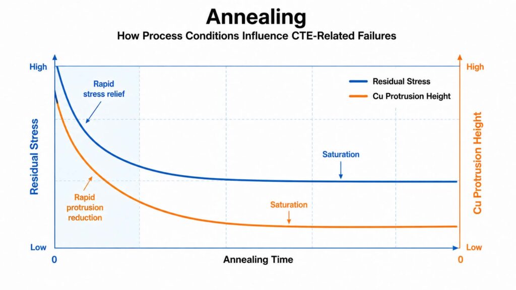
Post-plating annealing is a normal part of TGV processing — it stabilizes the electroplated copper’s microstructure and relieves some of the residual stress introduced during plating. But annealing is a double-edged process step: while moderate annealing reduces residual stress, prolonged annealing at high temperature (some studies use temperatures approaching 400-420°C) can generate new residual tensile stress in the glass as the structure cools back down, which is exactly the kind of stress that drives radial cracking. In other words, annealing is a mitigation for one failure mode (as-plated residual stress) that has to be carefully bounded to avoid triggering another (annealing-induced cracking).
Heating and Cooling Rate
Ramp rate shows up as a factor in more than one failure mode, and not always in the same direction. For radial crack formation during annealing, faster heating rates have been shown to increase crack probability, since the glass has less time to relax stress as it builds. For in-plane glass deformation near a via during thermal cycling, some studies have found the opposite relationship is protective — slower ramp rates reduce peak in-plane deformation, again because slower heating allows more time for stress relaxation before it accumulates to a damaging level. The common thread across both findings is the same: rapid temperature change gives a CTE-mismatched structure less time to redistribute stress, which tends to make things worse rather than better, regardless of which specific failure mode is being measured.
Design Strategies to Manage CTE Mismatch
Via Geometry and Copper Fill Volume
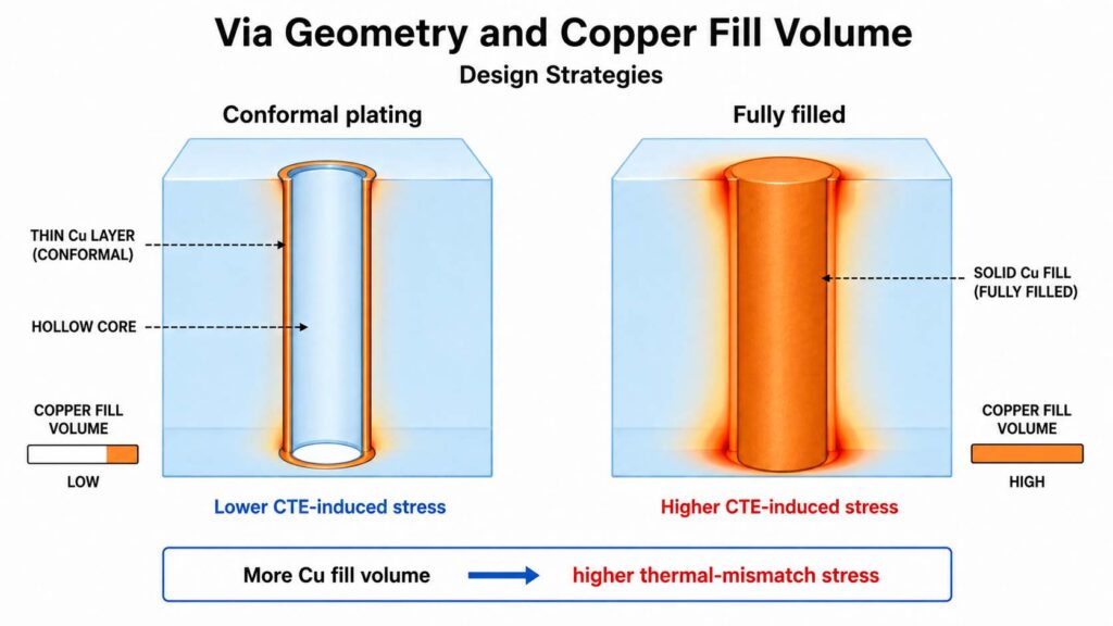
Since the stress driving these failures scales with how much copper is expanding against how much glass, reducing copper volume is one of the most direct levers available. A conformal plating approach — lining the via walls with copper rather than completely filling the via — uses substantially less copper than a full, void-free fill, and generally reduces the stress a via imposes on the surrounding glass, at the cost of higher via resistance compared to a fully filled via. Via taper also matters: a well-controlled, gradually tapered via profile helps distribute stress more evenly than an abrupt or irregular via wall, reducing localized stress concentration points where cracks are more likely to initiate.
Stress-Buffering and Buffer Layers
Where a design needs full copper fill for electrical reasons, adding a buffer or stress-relief layer between the copper and the glass — or between the TGV structure and the redistribution layer built on top of it — is a common mitigation. This kind of buffer layer specifically targets the edge-of-via and edge-of-RDL region, where finite element studies have identified some of the highest stress concentrations, and has been shown in some TGV structures to resolve cracking that would otherwise appear at the RDL edge.
RDL Design and Edge Clearance
Because panel-level warpage and edge cracking are connected to how many redistribution layers are stacked on the glass and how close circuitry sits to a panel or die edge, RDL design itself is a meaningful lever for CTE-related reliability. Keeping adequate clearance between circuit features and panel or die edges — some studies point to clearances in the range of a few hundred microns as meaningfully protective — reduces the risk that edge-concentrated stress propagates into a functional crack. Limiting the number of RDL layers, or balancing copper distribution across layers on both sides of the glass, reduces the number of CTE-mismatched interfaces the structure has to tolerate.
Testing and Predicting CTE-Related Reliability
Finite Element Modeling
Because via-level and panel-level thermal stress are difficult to measure directly and expensive to iterate on physically, finite element analysis (FEA) is the standard tool for predicting where stress will concentrate and how a given via geometry, fill strategy, or RDL layout will behave before it’s built. FEA models typically vary parameters like via aspect ratio, copper fill volume, RDL layer count, and edge clearance to identify which combinations keep predicted stress within the glass’s failure limits, and are commonly validated against physical measurements like digital image correlation (which tracks in-plane surface deformation during thermal cycling) or nanoindentation and atomic force microscopy (which characterize residual stress and copper protrusion after processing).
Thermal Cycling and Qualification Testing
Beyond modeling, TGV substrates are qualified through physical thermal cycling and stress tests — repeatedly cycling the substrate through a defined temperature range to accelerate the same failure mechanisms that would otherwise appear gradually over years of field use, alongside warpage measurements taken at the panel or package level. These tests follow the same general logic used across advanced packaging more broadly (temperature cycling and package warpage are both well-established test categories in semiconductor packaging qualification standards), applied specifically to the glass-copper interface that makes TGV reliability testing somewhat different from testing an all-silicon or all-organic structure.
CTE mismatch in a TGV isn’t a problem that gets solved once, by picking the right glass — it’s a condition that exists at every via, in every design, regardless of how well the bulk substrate is matched to the rest of the package. What determines whether that mismatch turns into a field failure is a combination of via geometry, copper fill strategy, annealing conditions, and RDL design, all of which give engineers real levers to pull even when the underlying physics — copper expanding faster than glass — can’t be changed. Treating CTE-related stress as an ongoing design and process variable, rather than a box that gets checked during material selection, is what separates a TGV substrate that survives years of thermal cycling from one that doesn’t.
FAQ
Why does CTE mismatch matter even if the glass substrate is well matched to silicon? Matching the bulk glass CTE to a silicon die or package addresses substrate-to-die stress, but it doesn’t address the separate mismatch between the glass and the copper filling its own vias. Copper’s CTE is far higher than any TGV glass composition, so local via-level stress exists regardless of how the bulk substrate is matched.
What is copper protrusion and why does it matter? Copper protrusion is the tendency of copper inside a via to expand and push out above the surrounding glass surface under heat, particularly after annealing. It matters because it can disrupt the surface flatness needed for redistribution-layer processing and is linked to the same residual-stress mechanisms that drive glass cracking.
Does slower heating always reduce CTE-related failures? Generally, yes — slower temperature ramps give a CTE-mismatched structure more time to relax stress, which has been shown to reduce both radial crack probability and in-plane glass deformation in different studies. The specific mechanism and ideal rate can vary by failure mode and process step, so ramp rate is typically optimized through testing rather than assumed.
How does reducing copper fill volume help reliability? Since via-level stress scales with how much copper is expanding against the surrounding glass, using less copper — for example, through conformal plating instead of a complete fill — generally reduces the stress imposed on the glass, though it comes with a trade-off of higher via resistance.
Is panel-level warpage the same problem as via-level cracking? They’re related but distinct. Via-level cracking and copper protrusion are driven by the local mismatch between copper and glass inside individual vias. Panel-level warpage is driven by mismatch between the glass core and the build-up/RDL layers across the whole substrate. Both stem from CTE mismatch, but they’re addressed with different design strategies.
What role does annealing play in TGV reliability? Annealing after copper plating relieves residual stress from the plating process, which is generally beneficial. But annealing at high temperature for extended periods can generate new residual tensile stress as the part cools, which can trigger cracking — so annealing conditions have to be tuned rather than simply maximized.
How is CTE-related TGV reliability tested before production? Primarily through finite element modeling to predict stress distribution and warpage under different design choices, validated against physical measurements such as digital image correlation, nanoindentation, or atomic force microscopy, followed by thermal cycling and warpage qualification testing on real substrates.
Can CTE mismatch in a TGV be eliminated entirely? Not with copper as the fill material — its CTE is simply too different from any practical TGV glass. Reliability engineering focuses on managing the resulting stress through via geometry, fill volume, buffer layers, and process conditions rather than eliminating the underlying mismatch.