Three numbers do most of the work in defining a TGV design: how wide each via is, how close together they can sit, and how many fit into a given area. Diameter, pitch, and density sound like simple geometry, but each one is constrained by a different discipline — diameter by what the formation and metallization process can reliably achieve, pitch by both glass mechanics and electrical coupling, and density by how those two combine with routing and power delivery needs. This guide walks through each parameter on its own terms, then looks at how they interact in practice.
Via Diameter: Setting the Baseline
What Determines Minimum and Maximum Diameter
Via diameter is the first parameter set in most TGV designs, and it’s bounded on both ends by process capability. On the small end, the via-formation method sets a practical floor: laser-based methods and photosensitive glass patterning can generally reach smaller diameters than mechanical or discharge-based methods, and different suppliers report achievable minimums anywhere from around 20 µm up to 30 µm or more, depending on their specific process. On the large end, there’s more flexibility — vias several hundred microns in diameter are common in applications like MEMS caps or sensor packaging, where routing density matters less than mechanical robustness or where the via itself needs to carry meaningful current.
Some processes support multiple via diameters on the same substrate, which lets a design use small, tightly packed vias for high-density signal routing in one region and larger vias for power delivery or structural connections elsewhere on the same panel.
Diameter’s Trade-off with Aspect Ratio and Resistance
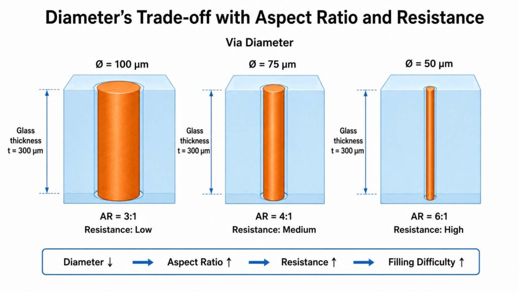
For a fixed glass thickness, a smaller via diameter means a higher aspect ratio (depth divided by diameter), and aspect ratio is one of the strongest drivers of how hard a via is to metallize reliably — seed layer coverage and void-free copper fill both get harder as aspect ratio climbs. That means diameter can’t be minimized in isolation; it has to be chosen alongside glass thickness and the metallization strategy the process can actually support at that combination. On the electrical side, a smaller diameter also means less copper cross-section, which raises via resistance — usually a secondary concern next to aspect ratio and fill quality, but one that matters more as via counts grow and cumulative resistance across many vias starts to affect power delivery.
Via Pitch: The Structural and Electrical Constraint
The Basic Structural Design Rule
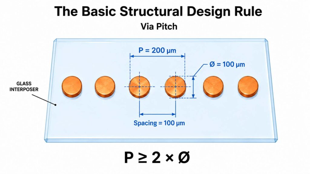
Pitch — the center-to-center spacing between adjacent vias — has a hard floor set by glass mechanics before electrical routing is even considered. A commonly cited baseline design rule is that via pitch should be at least twice the via diameter, which leaves a glass wall between adjacent vias roughly as wide as the via itself. That wall has to survive not just the initial via-formation and metallization process, but repeated thermal cycling afterward, so tighter pitch directly increases the risk of crack propagation between neighboring vias. A similar logic applies to the distance between a via and the edge of the substrate or die — edge clearance requirements in the range of a couple hundred microns are typical, both to protect the via itself and to reduce the risk of edge-originating cracks reaching it.
Why TGV Pitch Is Harder to Shrink Than TSV Pitch
Pitch is one of the areas where TGV currently trails TSV. Forming a fine-pitch via in glass is generally more difficult than forming an equivalent via in silicon, largely because glass etching processes — whether laser-based or wet-chemical — don’t scale down as predictably as silicon’s deep reactive-ion etching, and the metallization challenges (rough via-wall morphology, difficulty filling a tapered via completely) compound at tighter pitch. This is a meaningful practical distinction when comparing the two technologies for a design that specifically needs very high interconnect density: TSV currently supports finer pitch in production than TGV does, even though TGV can offer real advantages elsewhere.
Keep-Out Zones and Electrical Coupling at Tight Pitch
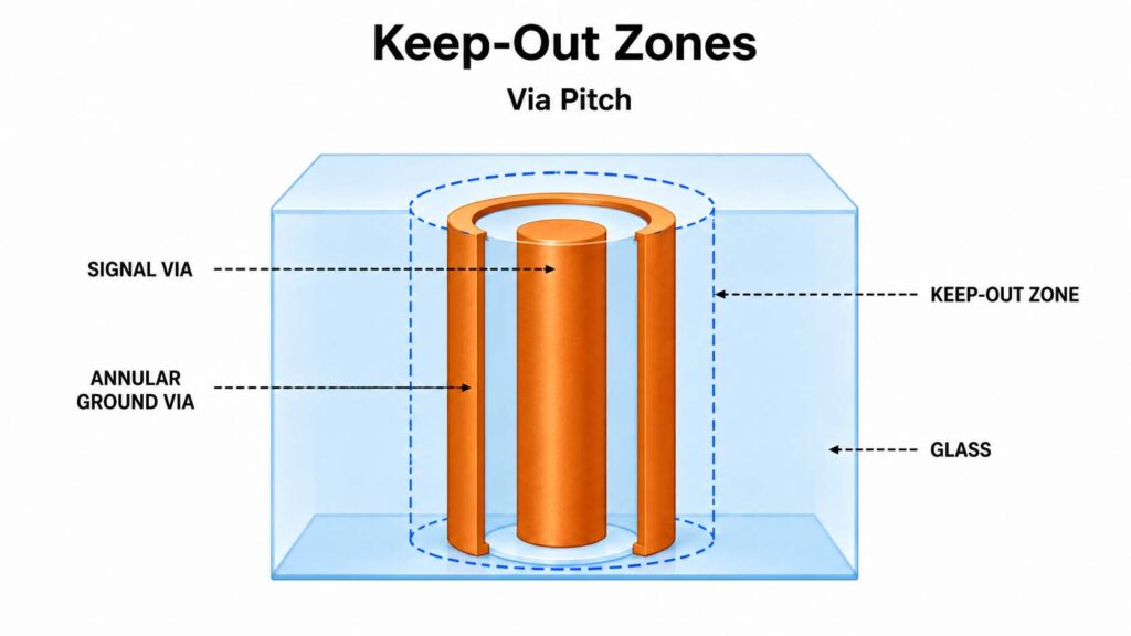
Beyond the structural floor, pitch is also shaped by electrical considerations that get more demanding as vias sit closer together. The keep-out zone (KOZ) concept — well established in TSV design, where the stress field around a copper-filled via can affect nearby active circuitry enough that a buffer distance has to be reserved around it — applies conceptually to TGV layout as well: via density is often limited less by how small a hole can physically be etched and more by how closely vias can sit without their surrounding stress fields or electrical coupling interfering with neighboring structures. At high frequencies specifically, closely spaced signal vias can couple to each other, increasing crosstalk and degrading insertion loss. Some high-frequency TGV designs address this directly by surrounding a signal via with a ring of grounded vias — a coaxial-like structure — and tuning via pitch, via radius, and the number of ground vias together to minimize signal loss and crosstalk at the target frequency, rather than choosing pitch purely from a mechanical or routing-density standpoint.
Via Density: Where Diameter and Pitch Combine
Density and Routing Capacity
Via density — the number of vias per unit area — is what diameter and pitch actually add up to in practice, and it’s the parameter that most directly determines how much I/O a given substrate area can support. High-density applications like AI accelerator interposers and HBM-style memory stacking need enough via density to route very large numbers of I/O connections through a compact area, which pushes designs toward the smallest diameter and tightest pitch the process can reliably support. Lower-density applications — many MEMS caps, simpler RF modules, or display driver interconnects — can use larger, more widely spaced vias, trading some routing density for a simpler, more robust, and generally lower-cost process.
Reported achievable via densities vary widely by process and application, with some advanced implementations cited in the thousands of vias per square millimeter — but these figures depend heavily on via diameter, pitch, and aspect ratio capability at a given supplier, so they’re better treated as an indication of what’s possible at the high end than as a general design target.
Density and Signal/Power Integrity
Beyond routing capacity, via density affects two other things that matter at the system level: power delivery network (PDN) integrity and signal crosstalk. A dense via array used for power and ground needs to provide a low-impedance return path for the signal vias running through the same region; where PDN impedance rises at resonance frequencies, insertion loss on nearby signal vias can increase and coupled noise can become a source of crosstalk in its own right. This means via density isn’t purely a routing-capacity question — the same density decisions that determine how much I/O fits in an area also shape how clean the electrical environment is for signals passing through that area, particularly as operating frequency increases.
Matching Parameters to the Application
Rather than treating diameter, pitch, and density as universal targets, it’s more useful to think of them as a design space that shifts depending on what the substrate needs to do:
| Application | Typical Via Diameter | Pitch Priority | Density Priority |
|---|---|---|---|
| AI accelerator / HPC interposers, chiplet integration | Small (tens of µm), often multiple sizes on one substrate | Tightest achievable, routing-density driven | High — I/O count is the primary constraint |
| RF and mmWave modules | Small to moderate | Set by electrical coupling and impedance as much as mechanics | Moderate, shaped by ground-via requirements |
| MEMS and sensor packaging | Larger (up to several hundred µm) | Looser, mechanical robustness prioritized | Low — a handful of vias per device is common |
| Display driver interconnects | Moderate to large, large panel format | Set by pixel pitch and panel routing needs | Moderate, spread across a large area |
The common thread is that diameter, pitch, and density aren’t independent dials — choosing an aggressive value for one usually tightens the constraints on the other two, and the right combination depends on whether the design is more limited by I/O count, by electrical performance at frequency, or by mechanical robustness in a specific application.
Getting TGV design parameters right is less about hitting the smallest possible numbers and more about understanding which constraint — process capability, glass mechanics, or electrical performance — is actually binding for a given application. A diameter chosen without considering aspect ratio and fill quality creates a metallization problem later; a pitch chosen without considering structural keep-out and crosstalk creates a reliability or signal-integrity problem later; and a density target set without considering PDN and routing congestion creates a design that looks good on paper but doesn’t route cleanly in practice. Treating the three as a connected system, rather than three separate numbers to optimize independently, is what turns a TGV design from a spec sheet into something that’s actually manufacturable and reliable.