AI accelerators, HPC processors, and chiplet-based designs have pushed packages to sizes and I/O densities that traditional organic substrates and even silicon interposers are starting to struggle with. Through-glass vias are at the center of one of the more promising answers to that problem: glass interposers and glass core substrates that route dense, high-frequency signals between chiplets while offering better warpage control at large package sizes than either silicon or organic alternatives. This guide looks specifically at how TGV fits into 2.5D and 3D integration — what it enables, where it still trails silicon, and why it’s gaining momentum now.
2.5D and 3D Integration: A Quick Primer
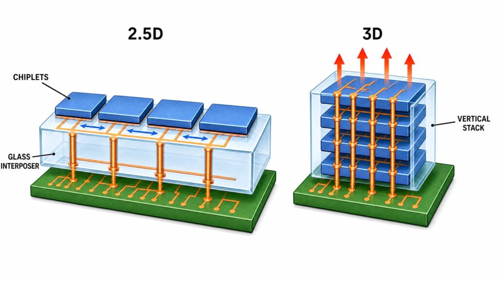
Side-by-Side vs. Stacked
2.5D integration places two or more separately fabricated dies next to each other on a shared interposer, which routes signals between them and down to the package substrate below. The dies themselves aren’t stacked — they sit side by side, connected laterally through the interposer’s redistribution layers and vias. 3D integration, by contrast, stacks dies vertically and connects them directly through vias running through the dies themselves, shortening the signal path even further at the cost of a more complex thermal and mechanical stack. Many real packages combine both approaches: a 3D-stacked memory module (like high-bandwidth memory) sitting alongside a large logic die, both mounted on a shared 2.5D interposer.
The Role of the Interposer
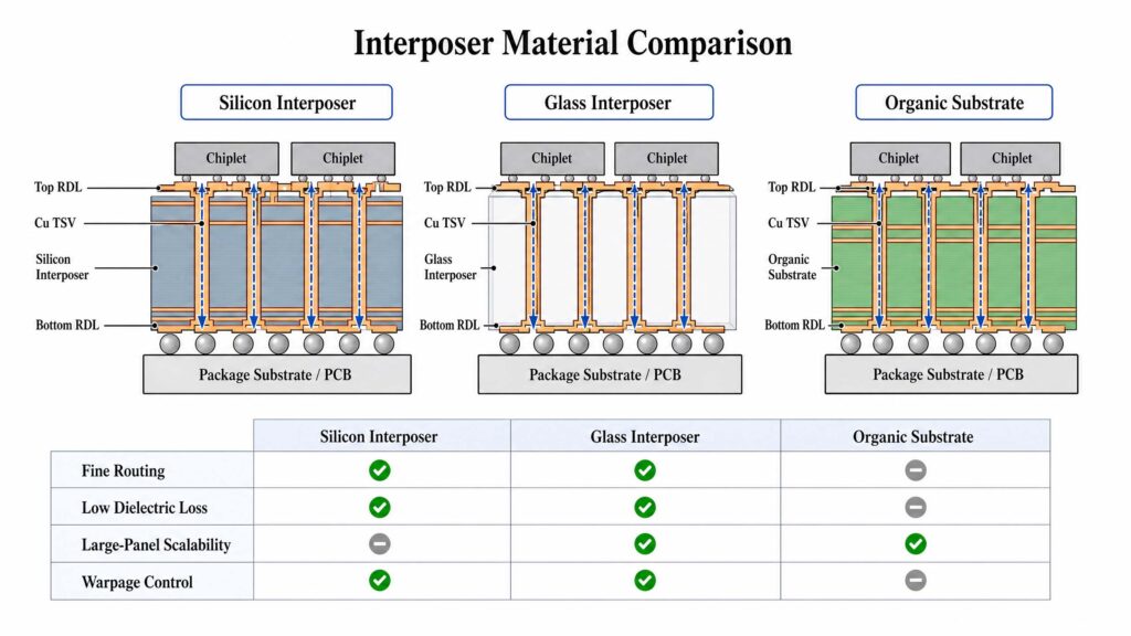
The interposer’s job in a 2.5D design is almost entirely about routing — taking the fine-pitch connections coming off each die and fanning them out to a coarser pitch the package substrate can handle, while also providing direct die-to-die connections that never need to leave the interposer at all. Interposers can be passive (routing only) or active (containing embedded logic), though passive interposers dominate current commercial designs; active interposers remain mostly confined to specialized cases like the base logic die in some HBM stacks. Whether the interposer is built from silicon, glass, or an organic material shapes what routing density, electrical performance, and substrate size are achievable — which is exactly where TGV-based glass interposers come in.
Where Glass and TGV Fit Into the Stack
Carrier, Interposer, Substrate: Three Entry Points
Glass is entering advanced packaging at more than one level simultaneously, which is part of why its adoption curve looks different from a typical new-material introduction. It’s already used, often without much fanfare, as a temporary carrier — providing stiffness and flatness for handling thin, fragile die stacks during fan-out and 3D assembly steps, without needing TGVs at all. Separately, glass with TGVs is used as an interposer — the routing layer between chiplets and the package substrate, playing the same structural role a silicon interposer plays today. And increasingly, glass is being adopted as a core substrate material, replacing the organic build-up films that have traditionally formed the structural base of a package substrate. These three entry points reinforce each other: equipment, process knowledge, and supply chain investment developed for glass as a carrier carries over to glass as an interposer or substrate, which is one reason the ecosystem around glass in packaging has matured faster than a typical new material transition.
Glass vs. Silicon Interposer for 2.5D Routing
As a routing layer, glass and silicon interposers do fundamentally the same job — dense vias plus fine redistribution layers connecting chiplets to each other and to the substrate below. Silicon interposers currently lead in absolute routing fineness: production silicon interposer processes have demonstrated line/space geometries down to a fraction of a micron with microbump pitches in the tens of microns. Glass interposer research and early production processes are close behind on these numbers and, in some published comparisons, achieve lower RDL capacitance and lower crosstalk than an equivalent silicon interposer at similar geometries, largely because glass’s lower dielectric constant reduces the parasitic coupling that silicon’s semiconducting bulk introduces. In practice, this means glass isn’t necessarily aiming to out-shrink silicon on raw geometry — it’s aiming to deliver comparable or better electrical performance at a lower cost and larger achievable size.
What Glass Interposers Enable That Silicon Doesn’t
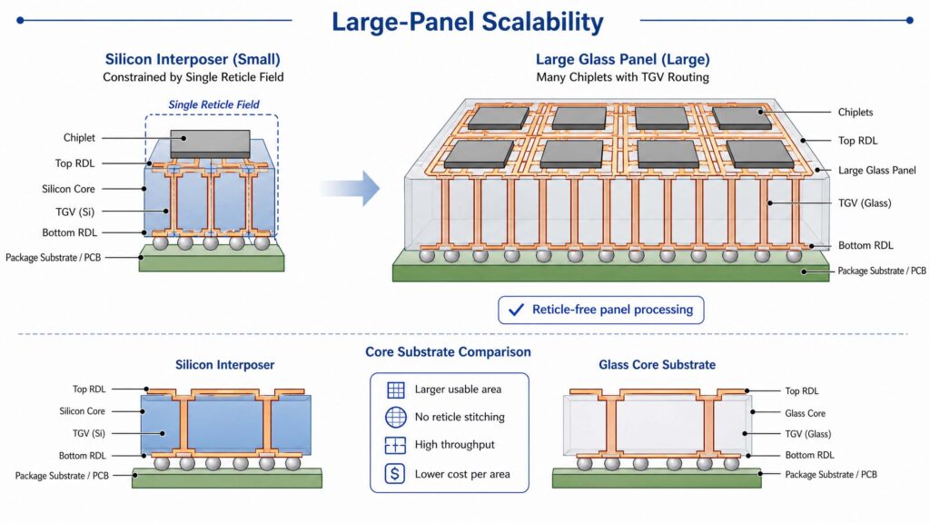
Larger Substrate Area Without Reticle Stitching
Silicon interposers are built using standard semiconductor lithography, which means their maximum size is constrained by the photolithography stepper’s reticle field — roughly the size of a single exposure field, on the order of a few centimeters per side. Building a larger interposer requires stitching multiple reticle fields together, which adds cost and complexity. Glass panels don’t have this constraint in the same way; large-format glass processing, already well developed in the display industry, allows TGV-based interposers and substrates to be built at panel sizes well beyond a single silicon reticle. As AI and HPC packages grow to accommodate more chiplets and larger high-bandwidth-memory stacks, this reticle-free scalability becomes one of glass’s most concrete practical advantages.
Embedding Dies Directly in the Glass
Some glass interposer processes go a step further than routing alone: they support forming cavities in the glass and embedding dies directly inside them, flush with or recessed into the substrate surface, with additional chiplets then mounted on top in a conventional flip-chip arrangement. This effectively blends 2.5D and 3D integration on a single substrate — some dies sit embedded within the glass itself, others sit stacked above it — and it’s a capability that isn’t naturally available with a standard silicon interposer, where dies mount on the surface rather than inside the interposer material.
Lower RDL Loss and Crosstalk at High Bus Widths
Chiplet-to-chiplet communication in a modern AI package increasingly looks like a high-speed serial link problem as much as a packaging problem — wide buses running at tens of gigabits per second per lane, where every bit of RDL loss and crosstalk translates directly into higher power consumption and lower achievable bandwidth. Glass’s lower dielectric loss compared to silicon, carried over from the same material properties that make TGV attractive for RF applications, gives chiplet-to-chiplet interconnects on a glass interposer a real efficiency advantage at these speeds — generally supporting wider buses, lower energy per bit, and longer achievable interconnect distances within the package than an equivalent silicon-routed link.
The Thermal Trade-off in 3D Stacks
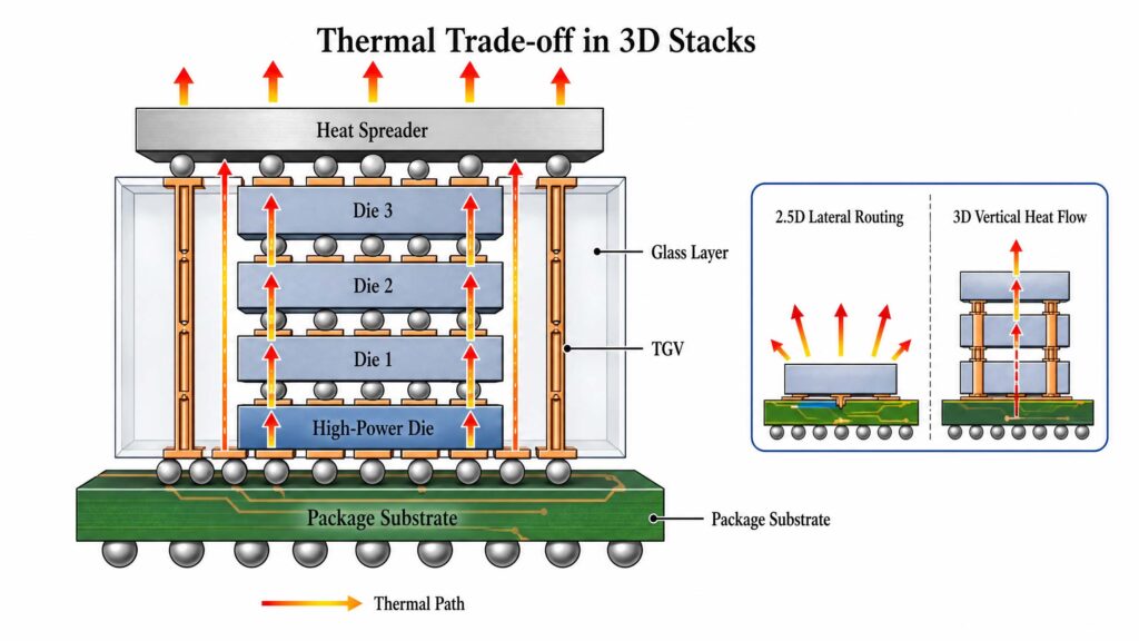
Glass’s advantages come with a trade-off that matters more in 3D stacking than in 2.5D routing: glass has meaningfully lower thermal conductivity than silicon. In a purely lateral 2.5D layout, where the interposer’s main job is routing rather than conducting heat vertically, this matters less — heat from each die can be extracted primarily through the top of the package, and the interposer’s thermal path isn’t the dominant concern. In a 3D stack, though, where dies are directly on top of one another and heat generated by a lower die has to move up through everything above it, an interposer or core layer with lower thermal conductivity is a more meaningful constraint. This is part of why glass adoption has moved faster in 2.5D interposer and substrate roles than in fully 3D-stacked configurations, and why designs that do combine glass with 3D stacking often pair it with dedicated thermal management features — embedded thermal vias, direct integration with heat spreaders, or careful floorplanning that keeps the highest-power dies on the most direct thermal path rather than buried under other layers.
Why This Matters Now: AI and HPC Package Scaling
The reason TGV and glass substrates are getting serious attention right now, rather than five years ago, comes down to package size and warpage. AI accelerator and HPC packages have grown to integrate more chiplets across a larger substrate area than earlier generations of packaging ever needed to handle, and organic build-up cores — the traditional structural material under most advanced packages — start to warp unacceptably at these larger sizes, because their polymer-based composition has a relatively low modulus and a CTE that doesn’t hold up well as panel area increases. Glass’s higher modulus and lower, more controllable CTE address that warpage problem directly, which is why glass core substrates are increasingly discussed not as a routing-layer alternative to silicon interposers specifically, but as a structural alternative to organic substrate cores more broadly — a shift that happens to bring TGV-based routing along with it, since a glass core substrate needs TGVs to route signals through it in the first place.
TGV’s role in 2.5D and 3D integration isn’t about replacing silicon interposers everywhere overnight. It’s about addressing a specific, growing problem — packages that have outgrown what a single silicon reticle or a warpage-prone organic core can comfortably support — with a material that happens to bring lower electrical loss and tunable thermal expansion along with it. Where that problem exists, glass interposers and glass core substrates built around TGV are becoming a serious option; where it doesn’t, silicon interposers and organic substrates remain the more mature, proven choice. The direction of travel, though, points toward glass playing a larger role as AI and HPC packages keep growing in size and I/O density.
FAQ
What’s the difference between 2.5D and 3D integration? 2.5D integration places multiple dies side by side on a shared interposer that routes signals between them. 3D integration stacks dies vertically and connects them directly through vias running through the dies themselves, shortening interconnect length further but adding thermal and mechanical complexity.
Why are glass interposers gaining attention for AI and HPC packaging? AI and HPC packages have grown large enough that silicon interposers run into reticle-size limits and organic substrate cores start to warp unacceptably. Glass avoids the reticle constraint, since large glass panels aren’t tied to a single lithography exposure field, and its higher modulus and lower CTE control warpage better than organic cores at large sizes.
Can dies be embedded directly inside a glass interposer? Yes, in some processes. Cavities can be formed in the glass and dies embedded inside them, with additional chiplets mounted on top in a conventional flip-chip arrangement — effectively combining 2.5D and 3D integration on the same substrate, a capability that isn’t naturally available with a standard silicon interposer.
Is glass better than silicon for interposer routing? It depends on what’s being optimized. Silicon interposers currently lead in the absolute finest achievable line/space and microbump pitch in production. Glass interposers generally offer lower RDL capacitance, lower crosstalk, and lower dielectric loss at comparable geometries, which translates into efficiency advantages for high-speed chiplet-to-chiplet links even without beating silicon on raw geometric fineness.
Does glass work well in 3D stacked packages? Glass’s lower thermal conductivity compared to silicon is a more significant factor in 3D stacks, where heat has to move vertically through the stack, than in 2.5D layouts where the interposer’s main role is lateral routing. This is one reason glass adoption has progressed faster in 2.5D interposer and substrate roles than in fully 3D-stacked configurations, and why 3D designs using glass often add dedicated thermal management features.
What is a glass core substrate, and how is it different from a glass interposer? A glass interposer is a routing layer between chiplets and the package substrate, functionally similar to a silicon interposer. A glass core substrate uses glass as the structural base of the package substrate itself, replacing organic build-up core material — a role focused more on warpage control and mechanical stability at large panel sizes than on fine-pitch chiplet routing specifically, though the two roles can overlap in some designs.
Why can’t silicon interposers just be made larger to match glass? Silicon interposers are built using standard semiconductor lithography, which limits a single interposer to roughly the size of one photolithography reticle field. Building larger silicon interposers requires stitching multiple reticle exposures together, adding cost and complexity that glass, which doesn’t depend on the same lithography constraint, avoids.
Is TGV-based glass packaging already in production for AI and HPC chips? Glass is already in production use as a carrier material in some packaging flows, and glass interposers and glass core substrates are moving from advanced R&D and early production toward broader commercial adoption, driven largely by AI and HPC package scaling. It’s an active, fast-moving area rather than a fully mature, universally adopted technology at this point.